Electrical characteristics, Absolute maximum ratings, Dc parameters for standard voltage – Rainbow Electronics AT89C5131 User Manual
Page 152: 40 ° c to +85 ° c; v, 0v; v
152
AT89C5131
4136A–USB–03/03
Electrical Characteristics
Absolute Maximum Ratings
DC Parameters for Standard Voltage
T
A
= -40
°
C to +85
°
C; V
SS
= 0V; V
CC
= 5V
±
10%; F = 0 to 40 MHz
Ambient Temperature Under Bias:
I = industrial ........................................................-40
°
C to 85
°
C
Storage Temperature .................................... -65
°
C to + 150
°
C
Voltage on V
CC
from V
SS
......................................-0.5V to + 6V
Voltage on Any Pin from V
SS
.....................-0.5V to V
CC
+ 0.2V
Note:
Stresses at or above those listed under “Absolute
Maximum Ratings” may cause permanent damage to
the device. This is a stress rating only and functional
operation of the device at these or any other condi-
tions above those indicated in the operational
sections of this specification is not implied. Exposure
to absolute maximum rating conditions may affect
device reliability.
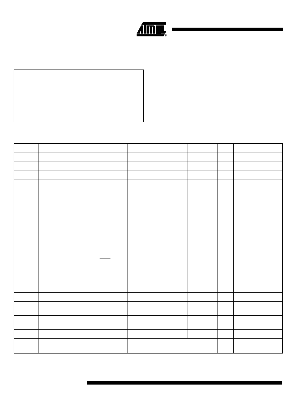
Symbol
Parameter
Min
Typ
(5)
Max
Unit
Test Conditions
V
IL
Input Low Voltage
-0.5
0.2Vcc - 0.1
V
V
IH
Input High Voltage except XTAL1, RST
0.2 V
CC
+ 0.9
V
CC
+ 0.5
V
V
IH1
Input High Voltage, XTAL1, RST
0.7 V
CC
V
CC
+ 0.5
V
V
OL
Output Low Voltage, ports 1, 2, 3 and 4
(6)
0.3
0.45
1.0
V
V
V
I
OL
= 100
µ
A
(4)
I
OL
= 1.6 mA
(4)
I
OL
= 3.5 mA
(4)
V
OL1
Output Low Voltage, port 0, ALE, PSEN
(6)
0.3
0.45
1.0
V
V
V
I
OL
= 200
µ
A
(4)
I
OL
= 3.2 mA
(4)
I
OL
= 7.0 mA
(4)
V
OH
Output High Voltage, ports 1, 2, 3, 4 and 5
V
CC
- 0.3
V
CC
- 0.7
V
CC
- 1.5
V
V
V
I
OH
= -10
µ
A
I
OH
= -30
µ
A
I
OH
= -60
µ
A
V
CC
= 5V
±
10%
V
OH1
Output High Voltage, port 0, ALE, PSEN
V
CC
- 0.3
V
CC
- 0.7
V
CC
- 1.5
V
V
V
I
OH
= -200
µ
A
I
OH
= -3.2 mA
I
OH
= -7.0 mA
V
CC
= 5V
±
10%
R
RST
RST Pulldown Resistor
20
40
200
k
Ω
I
IL
Logical 0 Input Current ports 1, 2, 3 and 4
-50
µ
A
V
IN
= 0.45V
I
LI
Input Leakage Current
±
10
µ
A
0.45V < V
IN
< V
CC
I
TL
Logical 1 to 0 Transition Current, ports 1, 2, 3
and 4
-650
µ
A
V
IN
= 2.0V
C
IO
Capacitance of I/O Buffer
10
pF
Fc = 1 MHz
T
A
= 25
°
C
I
PD
Power-down Current
100
200
µ
A
4.5V < V
CC
< 5.5V
(3)
I
CC
Power Supply Current
I
CCOP
= 0.7 Freq (MHz) + 3 mA
I
CCIDLE
= 0.6 Freq (MHz) + 2 mA
V
CC
= 5.5V
(1)(2)