Flash memory architecture – Rainbow Electronics AT89C5131 User Manual
Page 27
27
AT89C5131
4136A–USB–03/03
Table 31. External Data Memory Interface Signals
External Bus Cycles
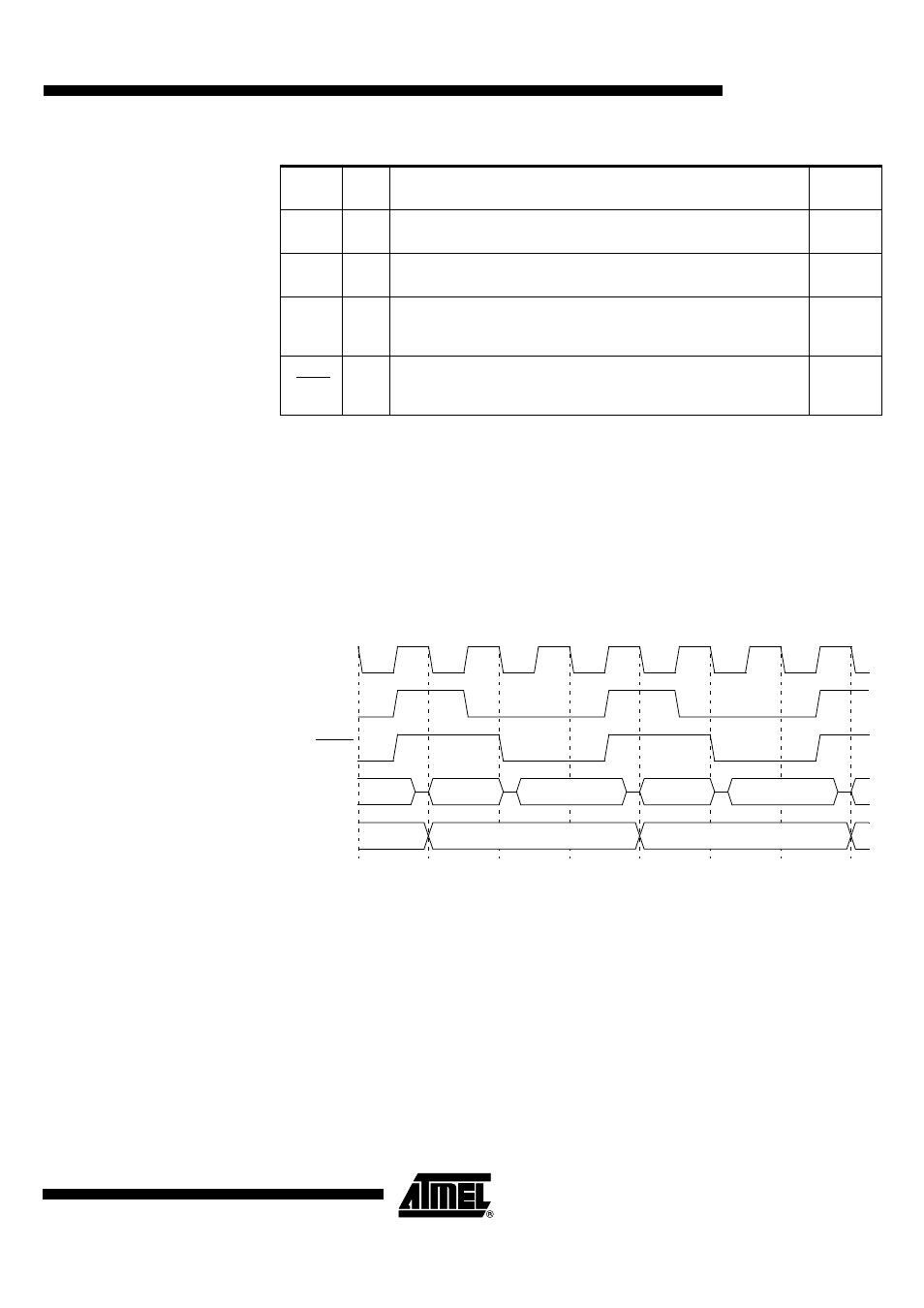
This section describes the bus cycles the AT89C5131 executes to fetch code (see
Figure 13) in the external program/code memory.
External memory cycle takes 6 CPU clock periods. This is equivalent to 12 oscillator
clock periods in standard mode or 6 oscillator clock periods in X2 mode. For further
information on X2 mode (see the clock Section).
For simplicity, the accompanying figure depicts the bus cycle waveforms in idealized
form and do not provide precise timing information.
Figure 13. External Code Fetch Waveforms
Flash Memory
Architecture
AT89C5131 features two on-chip Flash memories:
•
Flash memory FM0:
containing 32 Kbytes of program memory (user space) organized into 128-byte
pages,
•
Flash memory FM1:
3 Kbytes for bootloader and Application Programming Interfaces (API).
The FM0 supports both parallel programming and Serial In-System Programming (ISP)
whereas FM1 supports only parallel programming by programmers. The ISP mode is
detailed in the “In-System Programming” section.
All Read/Write access operations on Flash memory by user application are managed by
a set of API described in the “In-System Programming” section.
Signal
Name
Type
Description
Alternate
Function
A15:8
O
Address Lines
Upper address lines for the external bus.
P2.7:0
AD7:0
I/O
Address/Data Lines
Multiplexed lower address lines and data for the external memory.
P0.7:0
ALE
O
Address Latch Enable
ALE signals indicates that valid address information are available on lines
AD7:0.
-
PSEN
O
Program Store Enable Output
This signal is active low during external code fetch or external code read
(MOVC instruction).
-
ALE
P0
P2
PSEN
PCL
PCH
PCH
PCL
D7:0
D7:0
PCH
D7:0
CPU Clock