Flash memory status, Memory organization, Table 39 – Rainbow Electronics AT89C5131 User Manual
Page 39
39
AT89C5131
4136A–USB–03/03
The two lock bits provide different levels of protection for the on-chip code and data,
when programmed as shown to Table 39.
Table 39. Program Lock Bits of the SSB
Notes:
1. U: unprogrammed or "one" level.
2. P: programmed or “zero” level.
3. X: don’t care
4. WARNING: Security level 2 and 3 should only be programmed after Flash and code
verification.
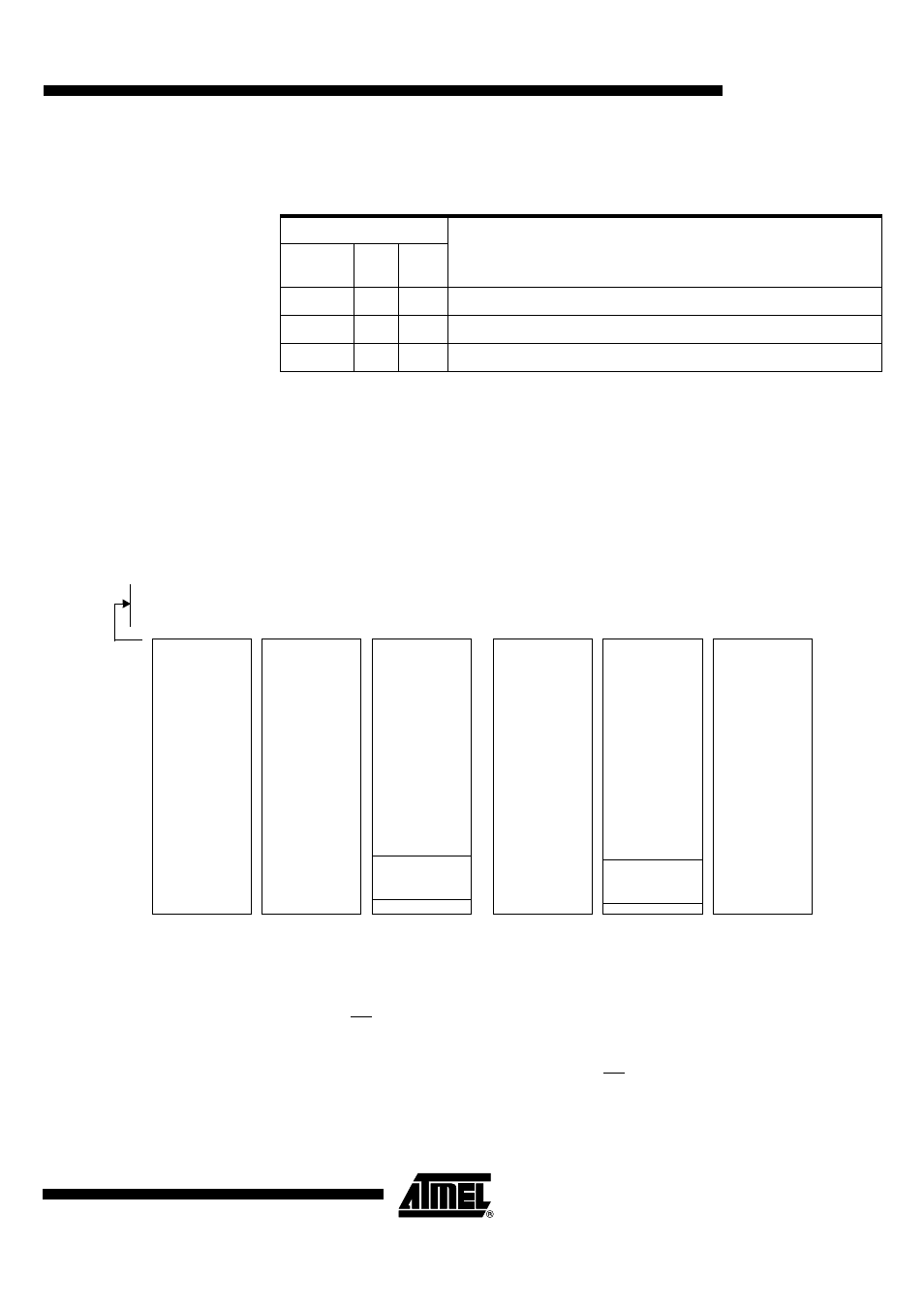
Flash Memory Status
AT89C5131 parts are delivered with the ISP boot in the Flash memory. After ISP or par-
allel programming, the possible contents of the Flash memory are summarized in Figure
19:
Figure 19. Flash Memory Possible Contents
Memory Organization
In the AT89C5131, the lowest 16K or 32K of the 64 Kbyte program memory address
space is filled by internal Flash.
When the EA is pin high, the processor fetches instructions from internal program Flash.
Bus expansion for accessing program memory from 16K or 32K upward is automatic
since external instruction fetches occur automatically when the program counter
exceeds 3FFFh (16K) or 7FFFh (32K). If the EA pin is tied low, all program memory
fetches are from external memory. If all storage is on chip, then byte location 3FFFh
(16K) or 7FFFh (32K) should be left vacant to prevent and undesired pre-fetch from
external program memory address 4000h (16K) or 8000h (32K).
Program Lock Bits
Protection Description
Security
Level
LB0
LB1
1
U
U
No program lock features enabled.
2
P
U
ISP programming of the Flash is disabled.
3
X
P
Same as 2, also verify through ISP programming interface is disabled.
0000h
Virgin
Default
Virgin
After ISP
After parallel
programming
After parallel
programming
After parallel
programming
Application
Application
After ISP
or
Dedicated
ISP
Dedicated
ISP
7FFFh AT89C5131
Application
Virgin
or
Application
Virgin
or
Application