Rainbow Electronics AT89C5131 User Manual
Page 8
8
AT89C5131
4136A–USB–03/03
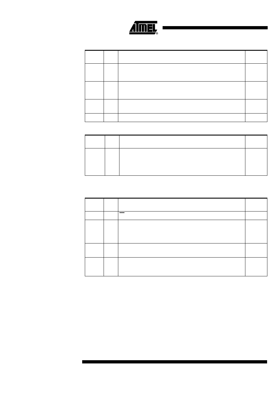
Table 5. LED Signal Description
Table 6. SPI Signal Description
T0
I
Timer Counter 0 External Clock Input
When Timer 0 operates as a counter, a falling edge on the T0 pin
increments the count.
P3.4
T1
I
Timer/Counter 1 External Clock Input
When Timer 1 operates as a counter, a falling edge on the T1 pin
increments the count.
P3.5
T2
I
O
Timer/Counter 2 External Clock Input
Timer/Counter 2 Clock Output
P1.0
T2EX
I
Timer/Counter 2 Reload/Capture/Direction Control Input
P1.1
Signal
Name
Type
Description
Alternate
Function
LED[3:0]
O
Direct Drive LED Output
These pins can be directly connected to the Cathode of standard LEDs
without external current limiting resistors. The typical current of each
output can be programmed by software to 2, 6 or 10 mA. Several outputs
can be connected together to get higher drive capabilities.
P3.3
P3.5
P3.6
P3.7
Signal
Name
Type
Description
Alternate
Function
SS
I/O
SS: SPI Slave Select
P1.1
MISO
I/O
MISO: SPI Master Input Slave Output line
When SPI is in master mode, MISO receives data from the slave
peripheral. When SPI is in slave mode, MISO outputs data to the master
controller.
P1.5
SCK
I/O
SCK: SPI Serial Clock
SCK outputs clock to the slave peripheral or receive clock from the master
P1.6
MOSI
I/O
MOSI: SPI Master Output Slave Input line
When SPI is in master mode, MOSI outputs data to the slave peripheral.
When SPI is in slave mode, MOSI receives data from the master controller
P1.7
Table 4. Timer 0, Timer 1 and Timer 2 Signal Description (Continued)
Signal
Name
Type
Description
Alternate
Function