Dc parameters for low voltage, 40 ° c to +85 ° c; v, 0v; v – Rainbow Electronics AT89C5131 User Manual
Page 153
153
AT89C5131
4136A–USB–03/03
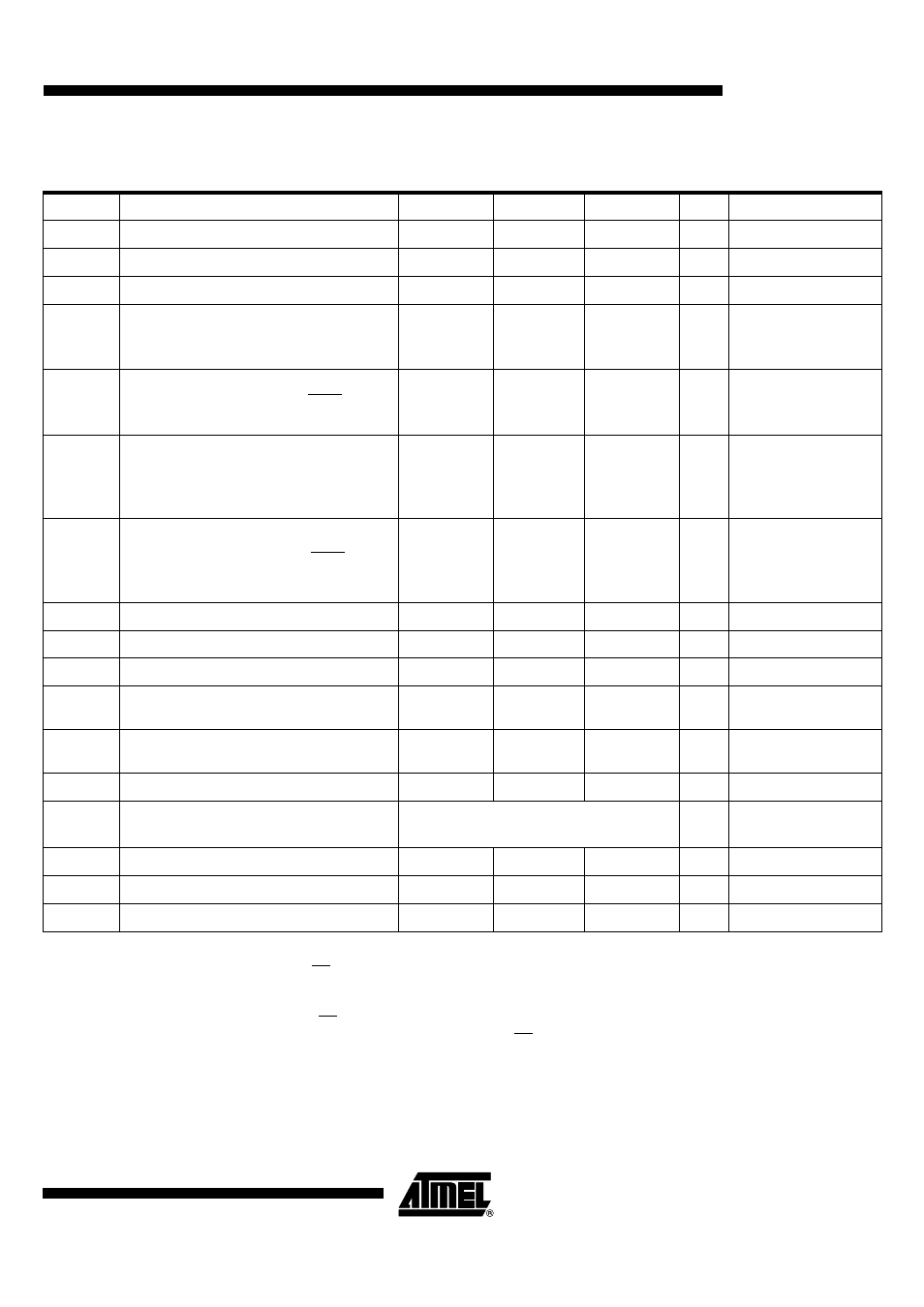
DC Parameters for Low Voltage
T
A
= -40
°
C to +85
°
C; V
SS
= 0V; V
CC
= 3.3V
±
10%; F = 0 to 40 MHz
Notes:
1. Operating I
CC
is measured with all output pins disconnected; XTAL1 driven with T
CLCH
, T
CHCL
= 5 ns (see Figure 69.), V
IL
=
V
SS
+ 0.5V,
V
IH
= V
CC
- 0.5V; XTAL2 N.C.; EA = RST = Port 0 = V
CC
. I
CC
would be slightly higher if a crystal oscillator used (see Figure
66.).
2. Idle I
CC
is measured with all output pins disconnected; XTAL1 driven with T
CLCH
, T
CHCL
= 5 ns, V
IL
= V
SS
+ 0.5V, V
IH
= V
CC
-
0.5V; XTAL2 N.C; Port 0 = V
CC
; EA = RST = V
SS
(see Figure 67).
3. Power-down I
CC
is measured with all output pins disconnected; EA = V
CC
, PORT 0 = V
CC
; XTAL2 NC.; RST = V
SS
(see Fig-
ure 68.). In addition, the WDT must be inactive and the POF flag must be set.
4. Capacitance loading on Ports 0 and 2 may cause spurious noise pulses to be superimposed on the V
OLS
of ALE and Ports 1
and 3. The noise is due to external bus capacitance discharging into the Port 0 and Port 2 pins when these pins make 1 to 0
transitions during bus operation. In the worst cases (capacitive loading 100 pF), the noise pulse on the ALE line may exceed
0.45V with maxi V
OL
peak 0.6V. A Schmitt Trigger use is not necessary.
5. Typicals are based on a limited number of samples and are not guaranteed. The values listed are at room temperature.
Symbol
Parameter
Min
Typ
(5)
Max
Unit
Test Conditions
V
IL
Input Low Voltage
-0.5
0.2Vcc - 0.1
V
V
IH
Input High Voltage except XTAL1, RST
0.2 V
CC
+ 0.9
V
CC
+ 0.5
V
V
IH1
Input High Voltage, XTAL1, RST
0.7 V
CC
V
CC
+ 0.5
V
V
OL
Output Low Voltage, ports 1, 2, 3 and 4
(6)
0.3
0.45
1.0
V
V
V
I
OL
= 100
µ
A
(4)
I
OL
= 0.8 mA
(4)
I
OL
= 1.6mA
(4)
V
OL1
Output Low Voltage, port 0, ALE, PSEN
(6)
0.3
0.45
1.0
V
V
V
I
OL
= 200
µ
A
(4)
I
OL
= 1.6 mA
(4)
I
OL
= 3.5 mA
(4)
V
OH
Output High Voltage, ports 1, 2, 3, 4 and 5
V
CC
- 0.3
V
CC
- 0.7
V
CC
- 1.5
V
V
V
I
OH
= -10
µ
A
I
OH
= -30
µ
A
I
OH
= -60
µ
A
V
CC
= 3.3V
±
10%
V
OH1
Output High Voltage, port 0, ALE, PSEN
V
CC
- 0.3
V
CC
- 0.7
V
CC
- 1.5
V
V
V
I
OH
= -200
µ
A
I
OH
= -1.6 mA
I
OH
= -3.5 mA
V
CC
= 3.3V
±
10%
R
RST
RST Pulldown Resistor
20
40
200
k
Ω
I
IL
Logical 0 Input Current ports 1, 2, 3 and 4
-50
µ
A
Vin = 0.45V
I
LI
Input Leakage Current
±
10
µ
A
0.45V < Vin < V
CC
I
TL
Logical 1 to 0 Transition Current, ports 1, 2, 3
and 4
-650
µ
A
Vin = 2.0V
C
IO
Capacitance of I/O Buffer
10
pF
Fc = 1 MHz
T
A
= 25
°
C
I
PD
Power-down Current
50
100
µ
A
3.0V < V
CC
< 3.6V
(3)
I
CC
Power Supply Current
I
CCOP
= 0.7 Freq (MHz) + 3 mA
I
CCIDLE
= 0.6 Freq (MHz) + 2 mA
V
CC
= 3.3V
(1)(2)
V
PFDP
Power Fail High Level Threshold
3.0
V
V
PFDM
Power Fail Low Level Threshold
2.2
V
Power fail hysteresis V
PFDP
- V
PFDM
0.15
V