Flash registers and memory map – Rainbow Electronics AT89C5131 User Manual
Page 36
36
AT89C5131
4136A–USB–03/03
Flash Registers and
Memory Map
The AT89C5131 Flash memory uses several registers:
•
Hardware registers can only be accessed through the parallel programming modes
which are handled by the parallel programmer.
•
Software registers are in a special page of the Flash memory which can be
accessed through the API or with the parallel programming modes. This page,
called “Extra Flash Memory”, is not in the internal Flash program memory
addressing space.
Hardware Registers
The only hardware registers of the AT89C5131 is called Hardware Security Byte (HSB).
Bootloader Jump Bit (BLJB)
One bit of the HSB, the BLJB bit, is used to force the boot address:
•
When this bit is set the boot address is 0000h.
•
When this bit is reset the boot address is F400h. By default, this bit is cleared and
the ISP is enabled.
Flash Memory Lock Bits
The three lock bits provide different levels of protection for the on-chip code and data,
when programmed as shown in Table 36.
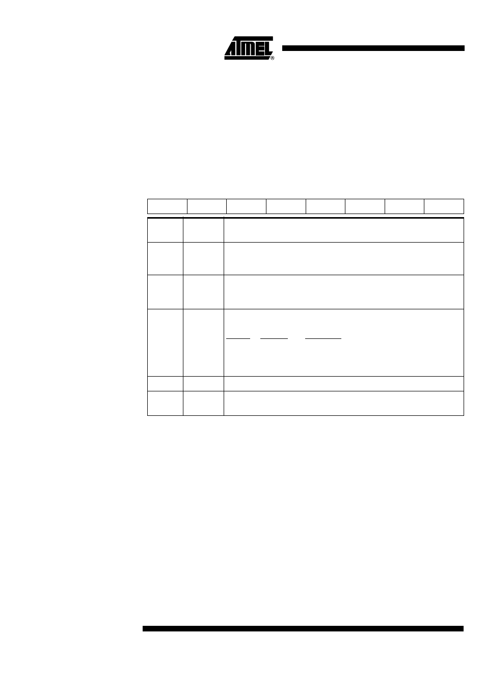
Table 35. Hardware Security Byte (HSB)
7
6
5
4
3
2
1
0
X2
BLJB
OSCON1
OSCON0
-
LB2
LB1
LB0
Bit
Number
Bit
Mnemonic
Description
7
X2
X2 Mode
Cleared to force X2 mode (6 clocks per instruction)
Set to force X1 mode, Standard Mode (Default).
6
BLJB
Bootloader Jump Bit
Set this bit to start the user’s application on next reset at address 0000h.
Cleared this bit to start the bootloader at address F400h (default).
5-4
OSCON1-0
Oscillator Control Bits
These two bits are used to control the oscillator in order to reduce consummation.
OSCON
OSCON0
Description
1
1
The oscillator is configured to run from 0 to 32 MHz
1
0
The oscillator is configured to run from 0 to 16 MHz
0
1
The oscillator is configured to run from 0 to 8 MHz
0
0
This configuration shouldn’t be set
3
-
Reserved
2-0
LB2-0
User Memory Lock Bits
See Table 36