Texas Instruments TMS380C26 User Manual
Page 91
TMS380C26
NETWORK COMMPROCESSOR
SPWS010A–APRIL 1992–REVISED MARCH 1993
POST OFFICE BOX 1443
•
HOUSTON, TEXAS
77251–1443
91
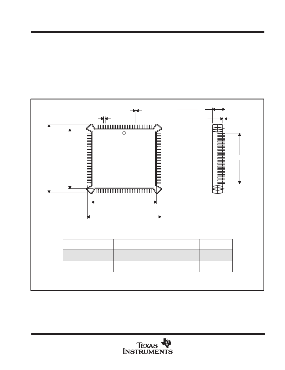
MECHANICAL DATA
JEDEC plastic leaded quad flat package (PQ suffix)
Each of these chip carrier packages consists of a circuit mounted on a lead frame and encapsulated within an
electrically nonconductive plastic compound. The compound withstands soldering temperatures with no
deformation, and circuit performance characteristics remain stable when the devices are operated in
high-humidity conditions. The packages are intended for surface mounting on solder lands on 0,635 (0.025)
centers. Leads require no additional cleaning or processing when used in soldered assembly.
0,635 (0.025) NOM
0,76 (0.030) NOM
0,254 (0.010) NOM
4,57 (0.180)
4,06 (0.160)
ALL LINEAR DIMENSIONS ARE IN MILLIMETERS AND PARENTHETICALLY IN INCHES
A
MIN
MAX
22,28
(0.877)
22,43
(0.883)
B
MIN
MAX
18,97
(0.747)
19,13
(0.753)
C
MIN
MAX
15,16
(0.597)
15,32
(0.603)
100
27,36
(1.077)
27,50
(1.083)
24,05
(0.947)
24,21
(0.953)
20,24
(0.797)
20,40
(0.803)
132
NO. OF
TERMINALS
JEDEC
OUTLINE
B
A
C
L
C
L
B
C
A
MO–069–AD
MO–069–AE