Texas Instruments TMS380C26 User Manual
Page 31
TMS380C26
NETWORK COMMPROCESSOR
SPWS010A–APRIL 1992–REVISED MARCH 1993
POST OFFICE BOX 1443
•
HOUSTON, TEXAS
77251–1443
31
PARAMETER MEASUREMENT INFORMATION
Outputs are driven to a minimum high-logic level of 2.4 volts and to a maximum low-logic level of 0.6 volts. These
levels are compatible with TTL devices.
Output transition times are specified as follows: For a high-to-low transition on either an input or output signal,
the level at which the signal is said to be no longer high is 2 volts, and the level at which the signal is said to be
low is 0.8 volts. For a low-to-high transition, the level at which the signal is said to be no longer low is 0.8 volts,
and the level at which the signal is said to be high is 2 volts, as shown below.
The rise and fall times are not specified but are assumed to be those of standard TTL devices, which are typically
1.5 ns.
0.8 V (Low)
2 V (High)
test measurement
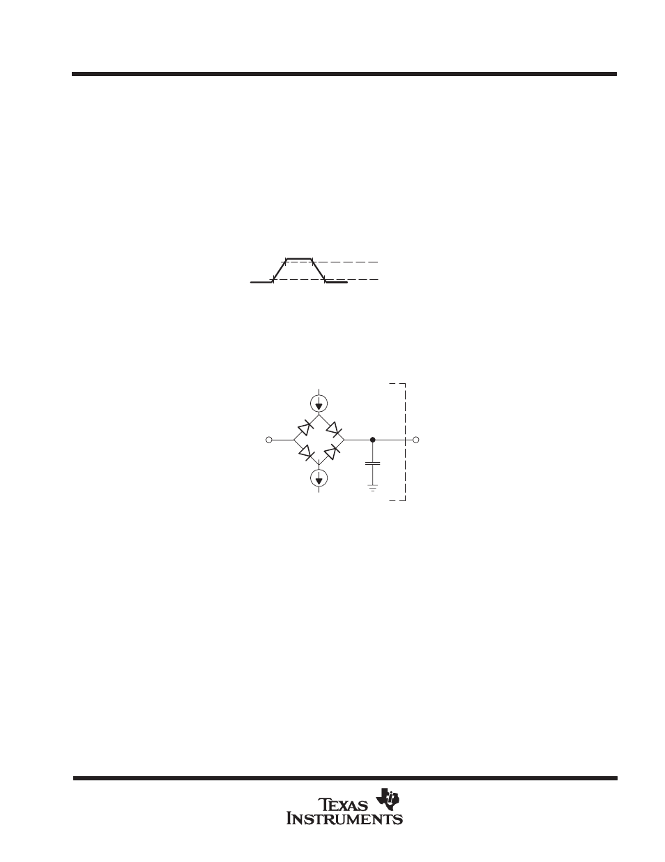
The test load circuit shown in Figure 4 represents the programmable load of the tester pin electronics which are
used to verify timing parameters of TMS380C26 output signals.
Output
Under
Test
Tester Pin
Electronics
IOL
IOH
CT
VLOAD
Where:
I
OL
= 2.0 mA DC level verification (all outputs)
I
OH
= 400
µ
A (all outputs)
V
LOAD
= 1.5 V typical DC level verification
0.7 V typical timing verification
C
T
= 65 pF typical load circuit capacitance
Figure 4. Test Load Circuit