Texas Instruments TMS380C26 User Manual
Page 55
TMS380C26
NETWORK COMMPROCESSOR
SPWS010A–APRIL 1992–REVISED MARCH 1993
POST OFFICE BOX 1443
•
HOUSTON, TEXAS
77251–1443
55
PARAMETER MEASUREMENT INFORMATION
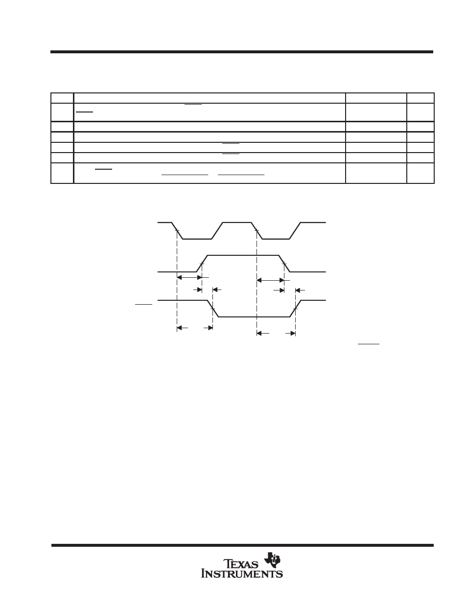
token ring — transmitter timing (see Figure 20)
NO.
PARAMETER
MIN
TYP
MAX
UNIT
159
Delay from DRVR rising edge (1.8 V) to DRVR falling edge (1.0 V) or DRVR falling edge (1.0 V) to
DRVR rising edge (1.8 V)
±
2
ns
160†
Delay from RCLK (or PXTALIN) falling edge (1.0 V) to DRVR rising edge (1.8 V)
(see Note 15)
161†
Delay from RCLK (or PXTALIN) falling edge (1.0 V) to DRVR falling edge (1.0 V)
(see Note 15)
162†
Delay from RCLK (or PXTALIN) falling edge (1.0 V) to DRVR falling edge (1.0 V)
(see Note 15)
163†
Delay from RCLK (or PXTALIN) falling edge (1.0 V) to DRVR rising edge (1.8 V)
(see Note 15)
164
DRVR/DRVR Asymmetry
t
d(DR)L
)
t
d(CRN)H
2
–
t
d(DR)H
)
t
d(DRN)L
2
±
1.5
ns
† When in active-monitor mode, the clock source is PXTALIN; otherwise, the clock-source is either RCLK or PXTALIN.
NOTE 15: This parameter is not tested to a minimum or a maximum but is measured and used as a component required for parameter 164.
DRVR
DRVR
RCLK or PXTALIN
161
0.60
1.50
2.40
0.60
1.50
2.40
0.60
1.50
2.60
160
162
163
159
159
Figure 20. Skew and Asymmetry from RCLK or PXTALIN to DRVR and DRVR