Texas Instruments TMS380C26 User Manual
Page 14
TMS380C26
NETWORK COMMPROCESSOR
SPWS010A–APRIL 1992–REVISED MARCH 1993
POST OFFICE BOX 1443
•
HOUSTON, TEXAS
77251–1443
14
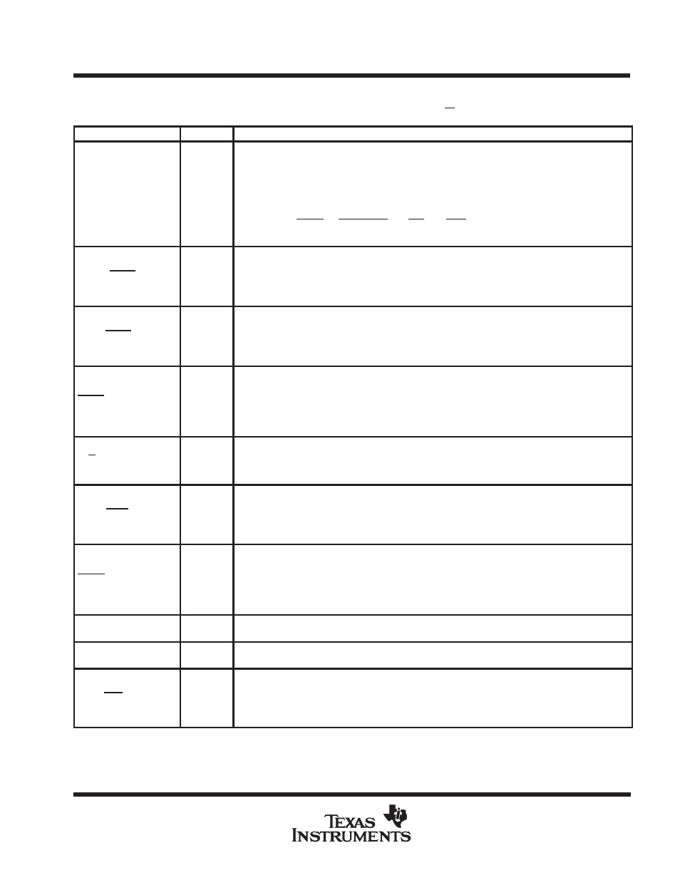
Terminal Functions (continued)
System Interface – Motorola Mode (SI/M = L)
PIN NAME
NO.
I/O
DESCRIPTION
SDDIR
38
OUT
System Data Direction. This output provides to the external data buffers a signal indicating the
direction in which the data is moving. During DIO writes and DMA reads, SDDIR is low (data direction
input to the TMS380C26). During DIO reads and DMA writes, SDDIR is high (data direction output
from the TMS380C26). When the system interface is
NOT involved in a DIO or DMA operation, then
SDDIR is high by default.
DATA
SDDIR
DIRECTION
DIO
DMA
H
output
read
write
L
input
write
read
SHLDA/SBGR
37
IN
System Bus Grant. This pin serves as an active-low bus grant, as defined in the standard 68000
interface, and is internally synchronized to SBCLK (see Note 1).
H = System bus not granted,
L
= System bus granted.
SHRQ/SBRQ
56
OUT
System Bus Request. This pin is used to request control of the system bus in preparation for a DMA
transfer. This pin is internally synchronized to SBCLK.
H = System bus not requested.
L
= System bus requested.
SIACK
24
IN
System Interrupt Acknowledge. This signal is from the host processor to acknowledge the interrupt
request from the TMS380C26.
H = System interrupt not acknowledged (see Note 1).
L
= System interrupt acknowledged: the TMS380C26 places its interrupt vector onto the system
bus.
SI/M
35
IN
System Intel/Motorola Mode Select. The value on this pin specifies the system interface mode.
H = Intel-compatible interface mode selected.
L
= Motorola-compatible interface mode selected. Motorola interface mode is always 16 bits.
SINTR/SIRQ
36
OUT
System Interrupt Request. TMS380C26 activates this output to signal an interrupt request to the host
processor.
H = No interrupt request.
L
= Interrupt request by TMS380C26.
SOWN
59
OUT
System Bus Owned. This signal indicates to external devices that TMS380C26 has control of the
system bus. This signal drives the enable signal of the bus transceiver chips, which drive the address
and bus control signals.
H = TMS380C26 does not have control of the system bus.
L
= TMS380C26 has control of the system bus.
SPH
62
I/O
System Parity High. The optional odd-parity bit for each address or data byte transmitted over
SADH0-SADH7 (see Note 1).
SPL
55
I/O
System Parity Low. The optional odd-parity bit for each address or data byte transmitted over
SADL0-SADL7 (see Note 1).
SRAS/SAS
39
I/O
Sytem Memory Address Strobe (see Note 3). This pin is an active-low address strobe that is an input
during DIO (although ignored as an address strobe) and an output during DMA.
H = Address not valid
L
= Address is valid and a transfer operation is in progress.
NOTES:
1. Pin has an internal pullup device to maintain a high voltage level when left unconnected (no etch or loads).
3. Pin should be tied to VCC with a 4.7-k
Ω
pullup resistor.