Qdrii, Qdrii+ –54 – Altera Stratix V Advanced Systems Development Board User Manual
Page 64
2–54
Chapter 2: Board Components
Memory
Stratix V Advanced Systems Development Board
January 2014
Altera Corporation
Reference Manual
QDRII+
Each FPGA device on the development board supports four burst-of-4 QDRII+ SRAM
memory devices for very-high-speed, low-latency memory access. The QDRII+ has a
x18 interface, providing device addressing for up to 72 Mb. Although the additional
address bit is available for future migration, the current board is populated with
36 Mb devices.
The QDRII+ has separate read and write data ports with DDR signaling at up to
550 MHz. A maximum theoretical bandwidth of over 158.4 Gbps for reading and
158.4 Gbps for writing is possible using eight interfaces (four interfaces per FPGA).
The pinout supports migration to extreme QDRII+ with a 667-MHz interface.
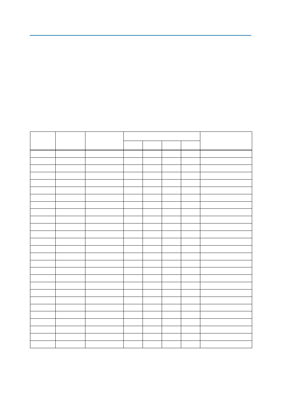
lists the QDRII+ pin assignments, signal names, and functions for FPGA1.
Table 2–25. FPGA1 QDRII+ Pin Assignments, Signal Names and Functions (Part 1 of 3)
Board
Reference
Schematic
Signal Name
I/O Standard
Stratix V GX FPGA1 Device Pin Number
Description
QDR2A
QDR2B
QDR2C
QDR2D
R9
A0
1.5-V HSTL Class I
BD19
AV11
B31
V34
Address bus
R8
A1
1.5-V HSTL Class I
BD17
AT12
C31
U35
Address bus
B4
A2
1.5-V HSTL Class I
AR18
AU9
R30
M36
Address bus
B8
A3
1.5-V HSTL Class I
AV16
AU11
E33
U32
Address bus
C5
A4
1.5-V HSTL Class I
AT18
AV10
M31
M39
Address bus
C7
A5
1.5-V HSTL Class I
AU17
AU10
J30
M37
Address bus
N5
A6
1.5-V HSTL Class I
AY19
AL11
C36
J36
Address bus
N6
A7
1.5-V HSTL Class I
BA18
AM13
B35
H36
Address bus
N7
A8
1.5-V HSTL Class I
BA16
AR13
B34
L35
Address bus
P4
A9
1.5-V HSTL Class I
AU16
AK12
D36
M33
Address bus
P5
A10
1.5-V HSTL Class I
AY18
AJ11
C34
K35
Address bus
P7
A11
1.5-V HSTL Class I
BA19
AN12
A35
K36
Address bus
P8
A12
1.5-V HSTL Class I
BC19
AR12
B32
K37
Address bus
R3
A13
1.5-V HSTL Class I
AN17
AJ12
T33
N31
Address bus
R4
A14
1.5-V HSTL Class I
AT17
AH12
T32
P33
Address bus
R5
A15
1.5-V HSTL Class I
AY16
AG12
C33
K34
Address bus
R7
A16
1.5-V HSTL Class I
BC17
AL12
A34
H37
Address bus
A9
A17
1.5-V HSTL Class I
AW17
AG10
D33
V33
Address bus
A3
A18
1.5-V HSTL Class I
AP16
AG11
P32
L36
Address bus
A10
A19
1.5-V HSTL Class I
AW16
AG9
D35
T35
Address bus (Unused)
B7
BWSN0
1.5-V HSTL Class I
AJ18
AF11
V30
K32
Write byte write select 0
A5
BWSN1
1.5-V HSTL Class I
AH18
AD14
W29
K31
Write byte write select 1
A1
CQ_N
1.5-V HSTL Class I
AG16
AP15
T30
R36
Echo clock
A11
CQ_P
1.5-V HSTL Class I
AY15
AU12
K30
J37
Echo clock
P10
D0
1.5-V HSTL Class I
AW19
BB11
B29
L32
Write data bus
N11
D1
1.5-V HSTL Class I
AV19
BC10
C30
M34
Write data bus
M11
D2
1.5-V HSTL Class I
AU19
AW11
A31
P34
Write data bus