Altera Stratix V Advanced Systems Development Board User Manual
Page 19
Chapter 2: Board Components
2–9
MAX V CPLD System Controller
January 2014
Altera Corporation
Stratix V Advanced Systems Development Board
Reference Manual
FLASH_A19
H15
1.8-V
FM address bus
FLASH_A20
H13
1.8-V
FM address bus
FLASH_A21
H16
1.8-V
FM address bus
FLASH_A22
J13
1.8-V
FM address bus
FLASH_A23
J16
1.8-V
FM address bus
FLASH_A24
G15
1.8-V
FM address bus
FLASH_A25
L16
1.8-V
FM address bus
FLASH_A26
E14
1.8-V
FM address bus
FLASH_D0
J14
1.8-V
FM data bus
FLASH_D1
J15
1.8-V
FM data bus
FLASH_D2
K16
1.8-V
FM data bus
FLASH_D3
N15
1.8-V
FM data bus
FLASH_D4
K15
1.8-V
FM data bus
FLASH_D5
N14
1.8-V
FM data bus
FLASH_D6
L14
1.8-V
FM data bus
FLASH_D7
L11
1.8-V
FM data bus
FLASH_D8
L15
1.8-V
FM data bus
FLASH_D9
L12
1.8-V
FM data bus
FLASH_D10
M16
1.8-V
FM data bus
FLASH_D11
L13
1.8-V
FM data bus
FLASH_D12
M15
1.8-V
FM data bus
FLASH_D13
M13
1.8-V
FM data bus
FLASH_D14
K14
1.8-V
FM data bus
FLASH_D15
P15
1.8-V
FM data bus
FMC_C2M_PG
E3
2.5-V
FMC carrier card to mezzanine module power good
FPGA1_CONF_DONE
A13
2.5-V
FPGA1 configuration done
FPGA1_CPU_RESETN
B1
2.5-V
FPGA1 reset
FPGA1_CVP_CONFDONE
N10
1.5-V
FPGA1 configuration via protocol done
FPGA1_DCLK
J3
2.5-V
FPGA1 configuration clock
FPGA1_FPP
A15
2.5-V
Configure FPGA1 via FPP at power up
FPGA1_MSEL0
A7
2.5-V
DIP switch for FPGA1 mode select 0
FPGA1_MSEL1
E1
2.5-V
DIP switch for FPGA1 mode select 1
FPGA1_MSEL2
A6
2.5-V
DIP switch for FPGA1 mode select 2
FPGA1_MSEL3
A12
2.5-V
FPGA1 mode select 3
FPGA1_MSEL4
A5
2.5-V
FPGA1 mode select 4
FPGA1_NCE
B3
2.5-V
FPGA1 chip enable
FPGA1_NCEO
F1
2.5-V
FPGA1 chip enable output
FPGA1_NCONFIG
K2
2.5-V
FPGA1 configuration active
FPGA1_NSTATUS
J4
2.5-V
FPGA1 configuration ready status
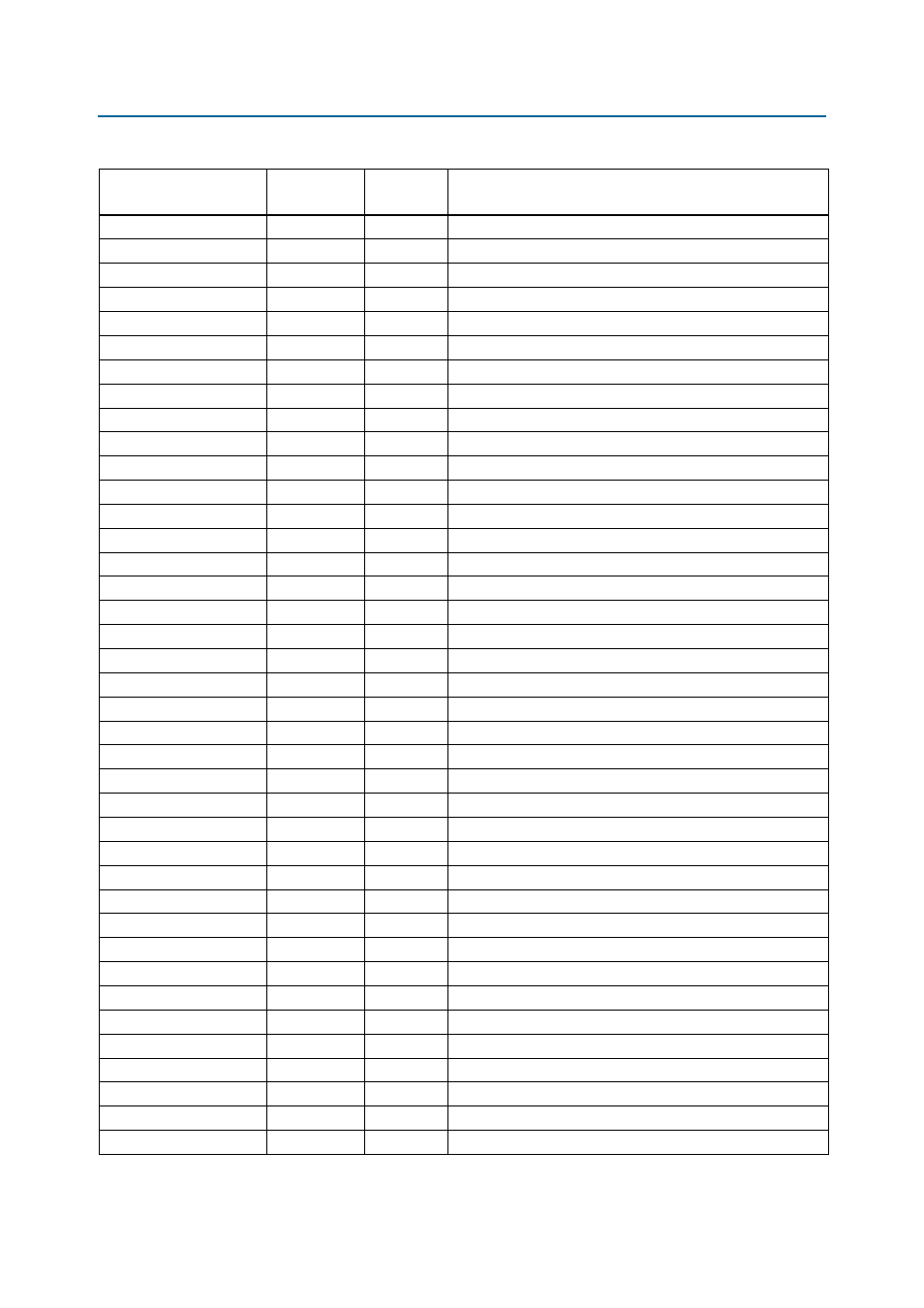
Table 2–4. MAX V CPLD System Controller Device Pin-Out (Part 2 of 5)
Schematic Signal Name
MAX V CPLD
Pin Number
I/O
Standard
Description