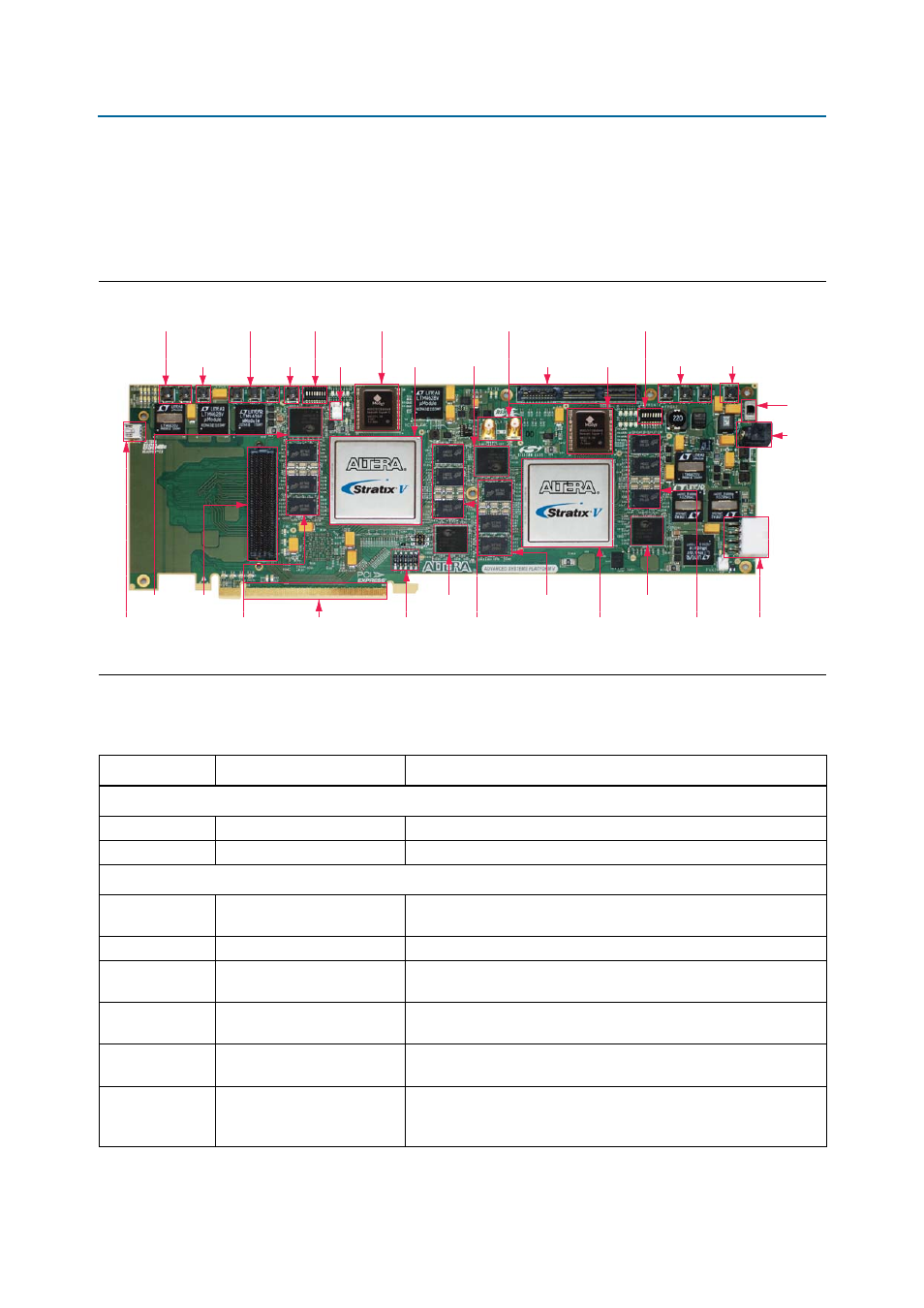
Board overview, Board overview –2, Figure 2–1 – Altera Stratix V Advanced Systems Development Board User Manual
Page 12: Table 2–1
2–2
Chapter 2: Board Components
Board Overview
Stratix V Advanced Systems Development Board
January 2014
Altera Corporation
Reference Manual
Board Overview
This section provides an overview of the Stratix V Advanced Systems development
board, including an annotated board image and component descriptions.
provides an overview of the development board features.
describes the components and lists their corresponding board references.
Figure 2–1. Overview of the Stratix V Advanced Systems Development Board Features
HSMC Port (J1) MoSys (U14)
MoSys (U4)
Power
Switch
(SW2)
12V-15 V
DC Input
Jack (J7)
QDRII+ x18
(U5)
QDRII+ x18
(U40)
QDRII+ x18
(U5)
QDRII+ x18
(U22)
DDR3 Memory x16
(U17, U24, U33)
DDR3 Memory x16
(U32, U39, U43)
DDR3 Memory x16
(U36, U21, U27)
DDR3 Memory x16
(U19, U30, U34)
ATX
Header (J9)
JTAG Header
(J11)
SMA Clock Input
Connector (J4, J5)
CPU Reset
Push Button
(S11)
CPU Reset
Push Button
(S7)
PCI Express
Edge Connector
(J13)
Fan Power
Header (J2)
On-Board
USB-Blaster II
Connector (J6)
Program Load,
Program Select
Push Button (S1, S2)
MAX V Reset
Push Button (S3)
Stratix V GX
FPGA (U29)
Stratix V GX
FPGA (U35)
General User
Push Button
(S8, S9, S10)
General User
Push Button
(S4, S5, S6)
User DIP Switch (SW3)
User DIP Switch
(SW1)
FMC (J8)
Table 2–1. Stratix V Advanced Systems Development Board Components (Part 1 of 4)
Board Reference
Type
Description
Featured Devices
U29, U35
FPGA
5SGXEA7N2F45C2N, 1932-pin BGA.
U73
CPLD
5M2210ZF256C4, 256-pin BGA.
Configuration, Status, and Setup Elements
J11
JTAG header
Provides access to the JTAG chain by using an external USB-Blaster
cable (disables the on-board USB-Blaster II).
J6
On-Board USB-Blaster II
Mini-USB 2.0 connector for programming and debugging the FPGA.
SW7
JTAG DIP switch
Enables and disables devices in the JTAG chain. This switch is located
on the back of the board.
SW5
FPGA1 mode select DIP
switch
Sets the Stratix V (U29) MSEL[2:0] pins. FPGA1 MSEL[4:3] = 10 on
the board.
SW6
FPGA2 mode select DIP
switch
Sets the Stratix V (U35) MSEL[2:0] pins. FPGA2 MSEL[4:3] = 10 on
the board.
SW4
Board settings DIP switch
Controls the MAX V CPLD System Controller functions such as clock
select, clock enable, and FPP configuration control. This switch is
located at the bottom of the board.