Fmc –33 – Altera Stratix V Advanced Systems Development Board User Manual
Page 43
Chapter 2: Board Components
2–33
Components and Interfaces
January 2014
Altera Corporation
Stratix V Advanced Systems Development Board
Reference Manual
FMC
The development board supports a FMC front-panel expansion for connectivity via
popular standards such as QSFP and SFP+. This low-pin count (LPC) FMC port (J8)
connects to the FPGA1 device. This interface provides 10 transceiver channels with
10.3125 Gbps capability. The FMC interface supports both single-ended and
differential signaling.
lists the FMC port pin assignments, signal names, and functions.
U47.J22
PCIE_RX_P9
1.4-V PCML
—
BA41
Receive data bus from PLX switch
U47.L22
PCIE_RX_P10
1.4-V PCML
—
AW41
Receive data bus from PLX switch
U47.M22
PCIE_RX_P11
1.4-V PCML
—
AY43
Receive data bus from PLX switch
U47.P22
PCIE_RX_P12
1.4-V PCML
—
AT43
Receive data bus from PLX switch
U47.R22
PCIE_RX_P13
1.4-V PCML
—
AP43
Receive data bus from PLX switch
U47.U22
PCIE_RX_P14
1.4-V PCML
—
AM43
Receive data bus from PLX switch
U47.V22
PCIE_RX_P15
1.4-V PCML
—
AK43
Receive data bus from PLX switch
U47.H20
PCIE_TX_N8
1.4-V PCML
—
AY40
Transmit data bus to PLX switch
U47.J20
PCIE_TX_N9
1.4-V PCML
—
AV40
Transmit data bus to PLX switch
U47.L20
PCIE_TX_N10
1.4-V PCML
—
AT40
Transmit data bus to PLX switch
U47.M20
PCIE_TX_N11
1.4-V PCML
—
AU42
Transmit data bus to PLX switch
U47.P20
PCIE_TX_N12
1.4-V PCML
—
AN42
Transmit data bus to PLX switch
U47.R20
PCIE_TX_N13
1.4-V PCML
—
AL42
Transmit data bus to PLX switch
U47.U20
PCIE_TX_N14
1.4-V PCML
—
AJ42
Transmit data bus to PLX switch
U47.V20
PCIE_TX_N15
1.4-V PCML
—
AG42
Transmit data bus to PLX switch
U47.H19
PCIE_TX_P8
1.4-V PCML
—
AY39
Transmit data bus to PLX switch
U47.J19
PCIE_TX_P9
1.4-V PCML
—
AV39
Transmit data bus to PLX switch
U47.L19
PCIE_TX_P10
1.4-V PCML
—
AT39
Transmit data bus to PLX switch
U47.M19
PCIE_TX_P11
1.4-V PCML
—
AU41
Transmit data bus to PLX switch
U47.P19
PCIE_TX_P12
1.4-V PCML
—
AN41
Transmit data bus to PLX switch
U47.R19
PCIE_TX_P13
1.4-V PCML
—
AL41
Transmit data bus to PLX switch
U47.U19
PCIE_TX_P14
1.4-V PCML
—
AJ41
Transmit data bus to PLX switch
U47.V19
PCIE_TX_P15
1.4-V PCML
—
AG41
Transmit data bus to PLX switch
Table 2–20. PCI Express Pin Assignments, Schematic Signal Names, and Functions (Part 3 of 3)
Board
Reference
(J13)
Schematic Signal
Name
I/O Standard
Stratix V GX
FPGA1 Device
Pin Number
Stratix V GX
FPGA2 Device
Pin Number
Description
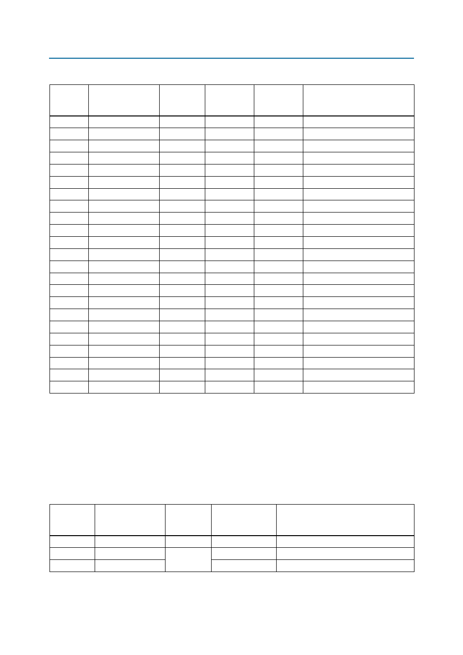
Table 2–21. FMC Port Pin Assignments, Schematic Signal Names, and Functions (Part 1 of 5)
Board
Reference
(J8)
Schematic Signal
Name
I/O Standard
Stratix V GX FPGA1
Device Pin Number
Description
D1
FMC_C2M_PG
3.3-V CMOS
—
Power good output
H4
FMC_CLK_M2C_P0
LVDS
J18
Differential clock input 0
H5
FMC_CLK_M2C_N0
H18
Differential clock input 0