Pcb layer stack-up, Figure 12-2 pcb layer stack-up (preliminary) – ADLINK aTCA-N700 User Manual
Page 76

aTCA-N700 HW Users Guide
76
12.2. PCB Layer Stack-up
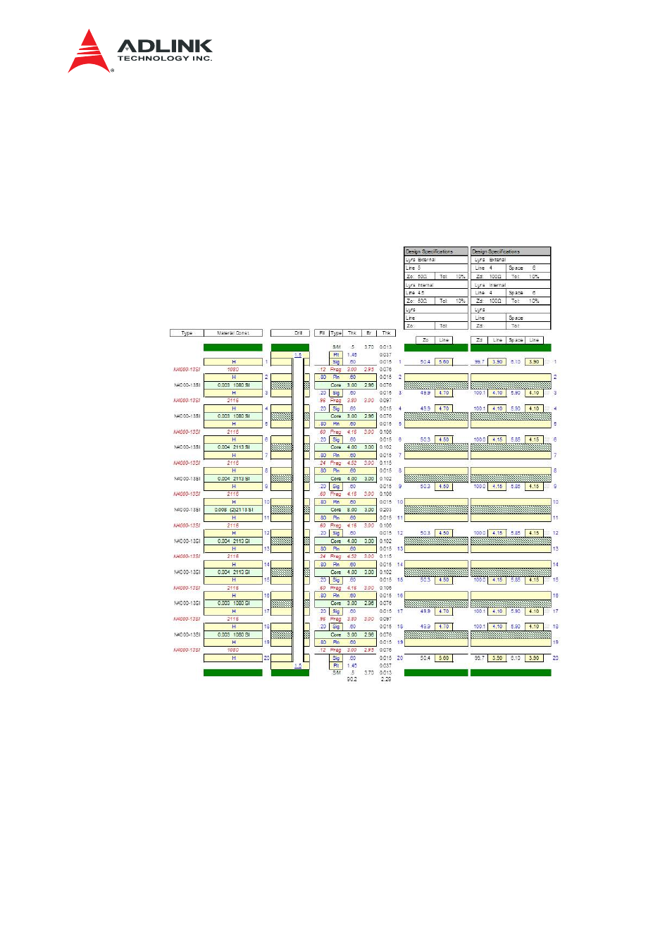
At the specified thickness of 2.45mm, a PCB may have around 20 internal layers. The blade is targeted to
have 20 layers of PCB laminate with a material compliant to a high speed, low loss epoxy such as
TU872SLK, which has a low dielectric constant (Dk ~ 3.6 at 10GHz) and low dissipation factor (Df ~ 0.008
at 10GHz). Figure 12-2 shows a layer stack-up example, which is subject to change.
Figure 12-2 PCB layer stack-up (preliminary)
See also other documents in the category ADLINK Hardware:
- USB-1901 (84 pages)
- USB-1210 (54 pages)
- USB-2401 (60 pages)
- USB-7230 (50 pages)
- USB-2405 (56 pages)
- DAQe-2010 (92 pages)
- DAQe-2204 (100 pages)
- DAQe-2213 (94 pages)
- DAQe-2501 (74 pages)
- PXI-2010 (84 pages)
- PXI-2020 (60 pages)
- PXI-2501 (62 pages)
- cPCI-9116 (98 pages)
- ACL-8112 Series (93 pages)
- ACL-8112 Series (94 pages)
- ACL-8112 Series (92 pages)
- ACL-8216 (75 pages)
- ACL-8111 (61 pages)
- PCM-9112+ (10 pages)
- PCM-9112+ (94 pages)
- cPCI-6216V (47 pages)
- ACL-6126 (28 pages)
- ACL-6128A (40 pages)
- PCM-6308V+ (4 pages)
- PCM-6308V+ (52 pages)
- PCI-7444 (82 pages)
- PCI-7434 (48 pages)
- PCI-7234 (56 pages)
- PCI-7260 (66 pages)
- PCI-7258 (38 pages)
- PCI-7256 (48 pages)
- PCI-7250 (48 pages)
- LPCI-7250 (48 pages)
- PCI-7396 (65 pages)
- PCI-7296 (59 pages)
- PCI-8554 (67 pages)
- PCIe-7360 (94 pages)
- PCIe-7350 (86 pages)
- PCIe-7300A (114 pages)
- PCIe-7200 (51 pages)
- PCI-7300A (112 pages)
- PCI-7300A (83 pages)
- PCI-7200 (96 pages)
- cPCI-7300 (82 pages)
- cPCI-7300 (83 pages)
