Local bus interface (ebi), Usb interface, Figure 8-8 p2041 local bus (ebi) interface – ADLINK aTCA-N700 User Manual
Page 49

aTCA-N700 HW Users Guide
49
• SATA
1.5Gbps/3.0Gbps
• Sustained sequential data read – up to 70MByte/sec at 128KB block size
• Sustained sequential data write – up to 60MByte/sec at 128KB block size
• 3.3V and 1.2V power supply
• 580mW
typical
• Integrated Voltage Detector to generate reset to prevent inadvertent writes
• Robust built-in ECC
• FBGA packet: 14.0 mm x 24.0 mm x 1.95 mm, 145-ball.
The GLS85LS1008P is a high performance, fully integrated solid state drive. It
combines an integrated SATA NAND flash memory controller and 8 GB of single-level
cell (SLC) NAND flash in a multi-chip package. Two of these are populated on the
board for redundancy purpose and used for OS and application image storage.
8.1.9. Local Bus Interface (EBI)
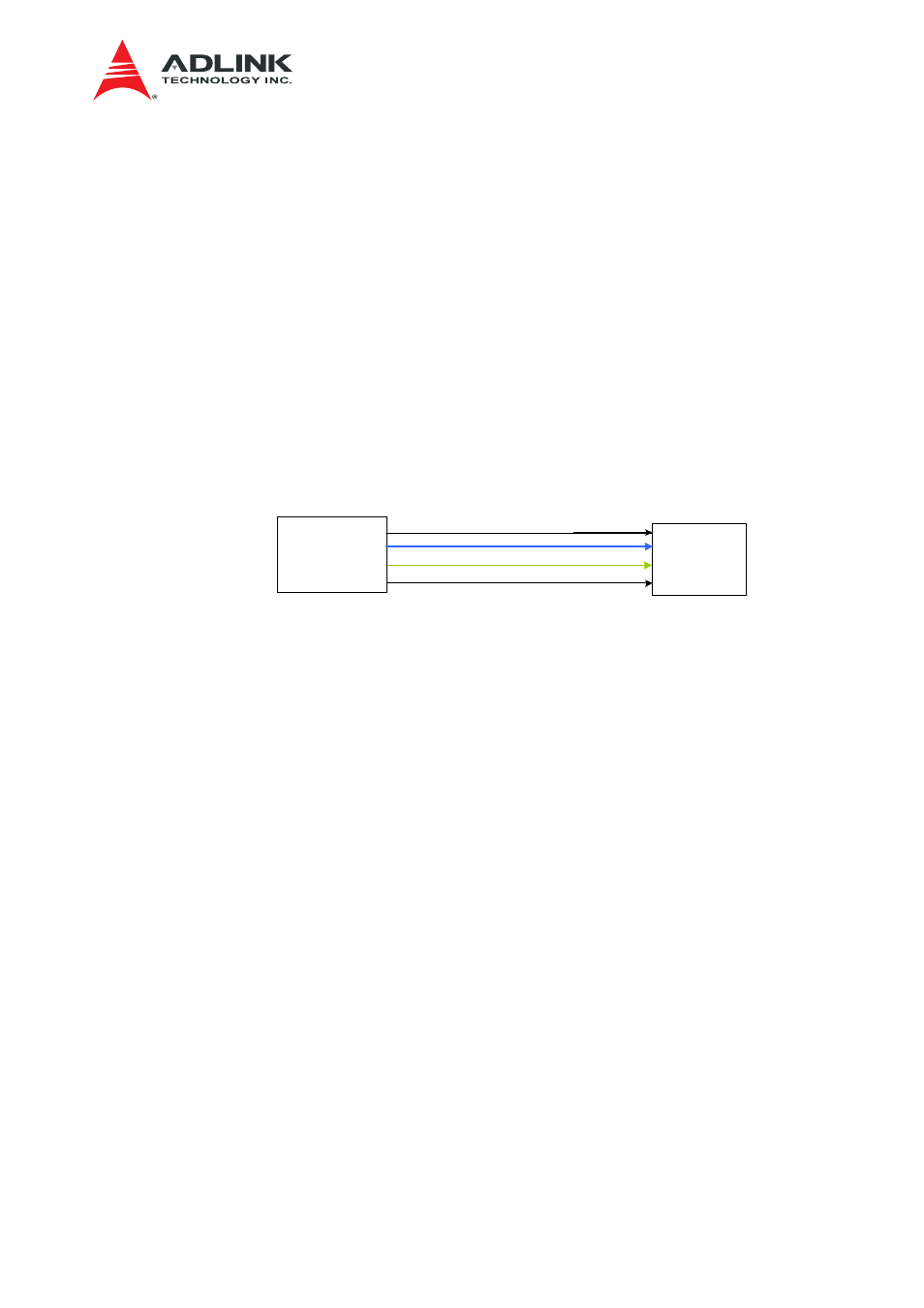
Illustrated in Figure 8-8 is the Local Bus Interface (EBI) block and its external
connections. The chip selects available for the local bus is LCS[3:0], but only LCS[3] is
used and connected to the system CPLD to access the CPLD registers.
LAD[15:0]
LA[31:27]
LCLK[1]
CPLD
D[7:0]
A[4:0]
CS#
LCLK
LCS[3]
Figure 8-8 P2041 Local Bus (EBI) Interface
Summarized below are selected features of the EBI interface:
• Support memory controller with eight memory banks
o
Variable memory block sizes(32Kbytes to 4Gbytes)
o
Selection of control signal generation on a per-bank basis
o
Data buffer controls activated on a per-bank basis
• General-purpose
chip-select
machine(GPCM)
o
Compatible
with
SRAM,EPROM,NOR Flash, EEPROM and peripherals
o
Global chip-select available at system reset.
o
Boot chip-select support for 8- and 16-bit devices.
o
Minimum three-clock access to external devices.
• NAND Flash control machine(FCM)
o
Compatible
with
small(512+16byte) and large(2048+64bytes) page
parallel NAND Flash EEPROM
o
Global chip-select available at system reset, with 4-Kbyte boot block
buffer for execute-in-place boot loading.
o
ECC checking enable/disable feature supported during boot.
o
Boot chip-select support for 8-bit devices.
o
Dual 2Kbyte/eight 512byte buffers allow simultaneous data transfer
during flash reads and programming.
• Three user-programmable machines(UPMs)
o
Support for 8- and 16-bit devices
o
Page mode support for successive transfers within a burst
o
Internal address multiplexing supporting 64-,128-,256- and 512Kbyte
and 1-,2-,4-,8-,16-,32-,64-,128- and 256Mbyte page banks
o
16-bit interface to peripherals
8.1.10. USB Interface
