Spi interface, Sata interface for chip ssd, Figure 8-7 p2041 spi interface – ADLINK aTCA-N700 User Manual
Page 48

aTCA-N700 HW Users Guide
48
8.1.7. SPI Interface
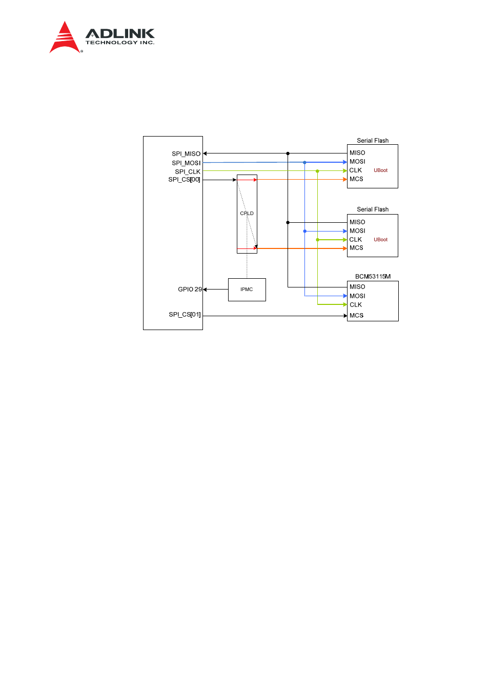
The SPI interface provides SPI_MOSI, SPI_MISO, SPI_CLK and four chip select
signals. Only two CSs are used on the board.
The SPI interface handles two serial flashes and the base switch, which is illustrated as
in
.
Figure 8-7 P2041 SPI Interface
The serial flashes contain the boot images and they are selected by the IPMC and
IPMC forwards the selection information to P2041 GPIO_3.
Summarized below are selected features of the SPI interface:
• Supports eSPI master.
• Supports RapidS full clock cycle operations
• Full-duplex or half-duplex master operation
• Supports Winbond dual output read
• Command in transaction level – easier for accessing eSPI devices
• Works with a range from 4-bit to 16-bit data characters
• Supports back-to-back character transmission and reception
• Supports
single-master
environment
• Maximum clock rate possible is (platform clock rate / 2)
• Independent programmable baud rate generator
• Programmable clock phase and polarity
• Support 4 different configurations per chip select
• Local loopback capability for testing
• Support booting from eSPI Interface.
8.1.8. SATA Interface for Chip SSD
The P2041 provides SATA1 and SATA2 interfaces through one of the external
configurable SerDes interfaces (Bank2 C and D). The SerDes interfaces SD_12 and
SD13 are connected to the two Chip SSD devices respectively to provide redundancy.
To enable this configuration, the Reset Code Word, RCW[SRDS_PRTCL] should be
set to 0x16 allowing three PCIe, two SGMIIs, and two SATAs for the external SerDes
interface mapping.
The Chip SSD used is GLS85LS1008P Industrial Grade SATA NANDrive are from
Greenliant. The features of the device are summarized as the following.
