Cn6880 embedded components, Figure 6-1 network processor subsystem – ADLINK aTCA-N700 User Manual
Page 26

aTCA-N700 HW Users Guide
26
Switch
Block
Optional mezzanine board
(TCAM)
LMP
NOR
Flash
72b 72b 72b 72b
CN6880 #1
(TOP)
RXAUI@2x
QLM0_[0:1]
RGM0
UART0
DIMM #1 (64b/72b, ECC)
LM
C3
x4
RJ-45
QL
M
3
PCIe@1x
Front
Faceplate
Serial
QLM0_[2:3]
QLM2_[0:3]
QLM4_[0:3]
RXAUI@2x
XAUI@4x
XAUI@4x
DIMM #2 (64b/72b, ECC)
DIMM #3 (64b/72b, ECC)
DIMM #4 (64b/72b, ECC)
LM
C2
LM
C1
LM
C0
BOOT
NOR
Flash
NOR
Flash
NAND
Flash
RGMII
QL
M
1
AD[31:0]
NOR
Flash
72b 72b 72b 72b
CN6880 #2
(BOTTOM)
RXAUI@2x
QLM0_[0:1]
RGM0
UART0
DDR3 VLP DIMM
32GB(4 x DIMM)
DIMM #1 (64b/72b, ECC)
LM
C
3
x4
RJ-45
QL
M
3
PCIe@1x
Serial
QLM0_[2:3]
QLM2_[0:3]
QLM4_[0:3]
RXAUI@2x
XAUI@4x
XAUI@4x
DIMM #2 (64b/72b, ECC)
DIMM #3 (64b/72b, ECC)
DIMM #4 (64b/72b, ECC)
LM
C
2
LM
C
1
LM
C
0
BOOT
NOR
Flash
NOR
Flash
NAND
Flash
RGMII
QL
M
1
AD[31:0]
DDR3 VLP DIMM
32GB(4 x DIMM)
TW
S
I1
TWS
I1
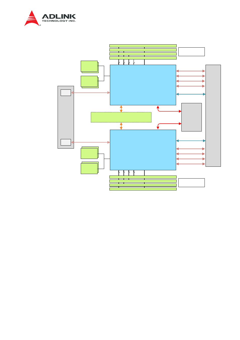
Figure 6-1 Network Processor Subsystem
6.1. CN6880 Embedded Components
Figure 6-2 illustrates the block diagram of the CN68XX devices. Detailed explanations can
be found in the “Cavium Networks OCTEON II CN68XX Hardware Reference Manual”.
The biggest customization on the board may be the data plane interfaces along with their
SerDes configurations. The CN6880 provides four internal SerDes blocks that can be
configured to provide different types of the interfaces, which will be covered in later sections.
The device has four internal DDR3 Memory Controllers (LMC0~LMC3) with four external
DDR3 SDRAM interfaces connected to these controllers. These DDR3 interfaces enable up
to 128GB of DDR3 memory installment or 32GB/Controller, if there are devices of enough
capacity.
