KEYENCE LK-CC100/DN100 User Manual
Page 48
3-12
3
3 Connecting to DeviceNet
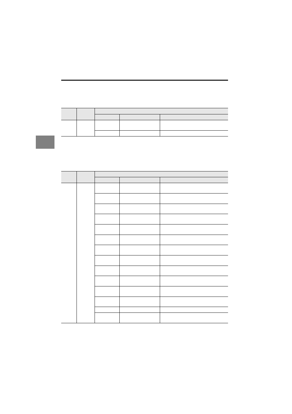
Output data buffer
The output data buffer refers to the area where parameters sent from the DeviceNet
master node to the LK-DN100 are stored.
A word is 16 bits.
Input control buffer
The input control buffer refers to the area where LK-DN100 statuses and responses to the
output control buffer control signals are stored.
LK-
DN100
Signal
direction
DeviceNet master node
Offset
Signal name
Explanation
Read
data
buffer
Word (14)
SET_PRG_NUM
Sets the program selection number from 0
to 7.
Word (15)
System reserved
LK-
DN100
Signal
direction
DeviceNet master node
Offset
Signal name
Explanation
Write
control
buffer
Bit (0)
CHG_PRG_ACQ
Turns ON (1) when the program number
changeover process completes.
Bit (1)
CHG_PRG_ERR
Turns ON (1) when an error occurs during
the program number changeover process.
Bit (2)
SYNC_TIM_ON_ACQ
Turns ON (1) when the synchronized timing
ON process completes.
Bit (3)
SYNC_TIM_ON_ERR
Turns ON (1) when an error occurs during
the synchronized timing ON process.
Bit (4)
SYNC_TIM_OFF_ACQ
Turns ON (1) when the synchronized timing
OFF process completes.
Bit (5)
SYNC_TIM_OFF_ERR
Turns ON (1) when an error occurs during
the synchronized timing OFF process.
Bit (6)
SYNC_ZERO_ON_ACQ
Turns ON (1) when the synchronized zero
ON process completes.
Bit (7)
SYNC_ZERO_ON_ERR
Turns ON (1) when an error occurs during
the synchronized zero ON process.
Bit (8)
SYNC_ZERO_OFF_ACQ Turns ON (1) when the synchronized zero
OFF process completes.
Bit (9)
SYNC_ZERO_OFF_ERR
Turns ON (1) when an error occurs during
the synchronized zero OFF process.
Bit (10)
SYNC_RESET_ACQ
Turns ON (1) when the synchronized reset
process completes.
Bit (11)
SYNC_RESET_ERR
Turns ON (1) when an error occurs during
the synchronized reset process.
Bit (12)
System reserved
Bit (13)
CHG_PRG_ENBLE
Turns ON (1) when program changeover is
possible.