Rainbow Electronics DS2180A User Manual
Page 6
DS2180A
041995 6/36
DATA I/O
Following the eight SCLK cycles that input an address/
command byte to write, a data byte is strobed into the
addressed register on the rising edges of the next eight
SCLK cycles. Following an address/command word to
read, contents of the selected register are output on the
falling edges of the next eight SCLK cycles. The SDO
pin is tri-stated during device write and may be tied to
SDI in applications where the host processor has a bidi-
rectional I/O pin.
BURST MODE
The burst mode allows all onboard registers to be con-
secutively read and written by the host processor. A
burst read is used to poll all registers; RSR contents will
be unaffected. This feature minimizes device initializa-
tion time on power-up or system reset. Burst mode is ini-
tiated when ACB.7 is set and the address nibble is 0000.
Burst is terminated by a low-high transition on CS.
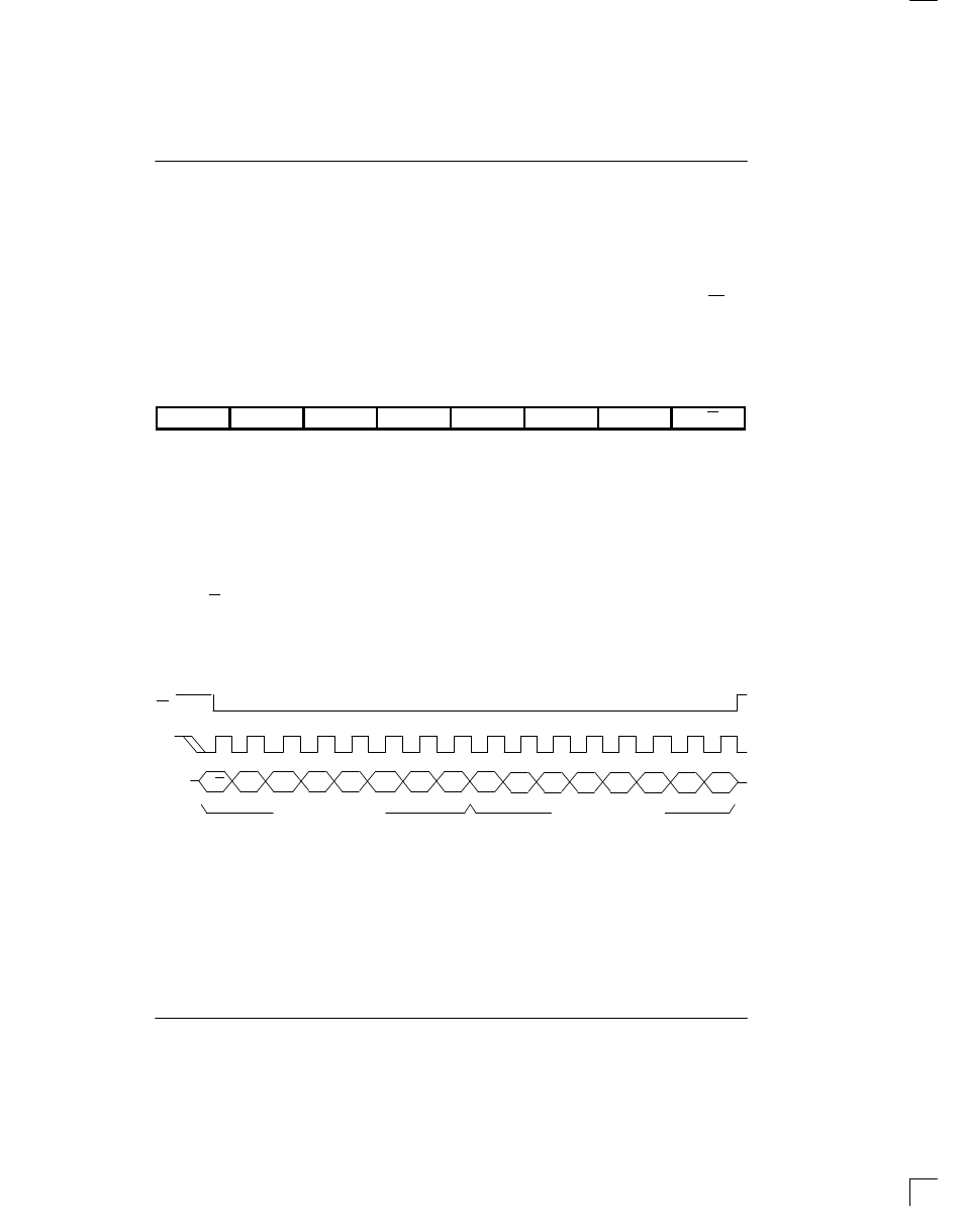
ACB: ADDRESS COMMAND BYTE Figure 2
(MSB)
(LSB)
BM
–
–
ADD3
ADD2
ADD1
ADD0
R/W
SYMBOL
POSITION
NAME AND DESCRIPTION
BM
ACB.7
Burst Mode. If set (and ACB.1 through ACB.4=0) burst read or write is en-
abled.
–
ACB.6
Reserved, must be 0 for proper operation.
–
ACB.5
Reserved, must be 0 for proper operation.
ADD3
ACB.4
MSB of register address.
ADD0
ACB.1
LSB of register address.
R/W
ACB.0
Read/Write Select.
0 = write addressed register.
1 = read addressed register.
SERIAL PORT READ/WRITE Figure 3
R/W
ADD0
ADD1
ADD2
0
0
BM
D0
D2
D3
D1
D4
D5
D6
D7
CS
SCLK
SDI
1
,SDO
2
ADDRESS/COMMAND
DATA INPUT/OUTPUT
ADD3
NOTES:
1. SDI sampled on rising edge of SCLK.
2. SDO updated on falling edge of SCLK.