Rainbow Electronics DS2180A User Manual
Page 5
DS2180A
041995 5/36
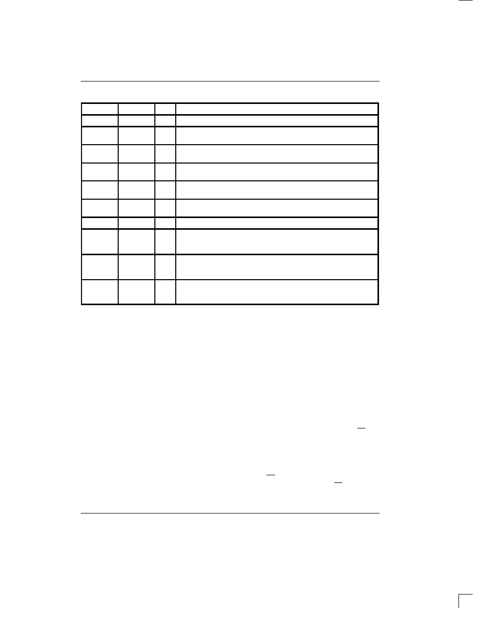
REGISTER SUMMARY Table 5
REGISTER
ADDRESS
T/R
1
DESCRIPTION/FUNCTION
RSR
0000
R
2
Receive Status Register. Reports all receive alarm conditions.
RIMR
0001
R
Receive Interrupt Mask Register. Allows masking of individual alarm-gen-
erated interrupts.
BVCR
0010
R
Bipolar Violation Count Register. 8-bit presettable counter which records
individual bipolar violations.
ECR
0011
R
Error Count Register. Two independent 4-bit counters which record OOF
occurrences and individual frame bit or CRC errors.
CCR
3
0100
T/R
Common Control Register. Selects device operating characteristics com-
mon to receive and transmit sides.
RCR
3
0101
R
Receive Control Register. Programs device operating characteristics
unique to the receive side.
TCR
3
0110
T
Transmit Control Register. Selects additional transmit side modes.
TIR1
TIR2
TIR3
0111
1000
1001
T
T
T
Transmit Idle Registers. Designate which outgoing channels are to be sub-
stituted with idle code.
TTR1
TTR2
TTR3
1010
1011
1100
T
T
T
Transmit Transparent Registers. Designate which outgoing channels are
to be treated transparently. (No robbed bit signaling or bit 7 zero insertion.)
RMR1
RMR2
RMR3
1101
1110
1111
R
R
R
Receive Mark Registers. Designate which incoming channels are to be re-
placed with idle or digital milliwatt codes (under control of RCR).
NOTES:
1. Transmit or receive side register.
2. RSR is a read only register; all other registers are read/write.
3. Reserved bit locations in the control registers should be programmed to 0 to maintain compatibility with future
transceiver products.
SERIAL PORT INTERFACE
Pins 14 through 18 of the DS2180A serve as a micropro-
cessor/microcontroller-compatible serial port. Sixteen
onboard registers allow the user to update operational
characteristics and monitor device status via host con-
troller, minimizing hardware interfaces. Port read/write
timing is unrelated to the system transmit and receive
timing, allowing asynchronous reads and/or writes by
the host.
ADDRESS/COMMAND
Reading or writing the control, configuration or status
registers requires writing one address command byte
prior to transferring register data. The first bit written
(LSB) of the address/command word specifies register
read or write. The following 4-bit nibble identifies regis-
ter address. The next two bits are reserved and must be
set to 0 for proper operation. The last bit of the address/
command word enables burst mode when set; the burst
mode causes all registers to be consecutively written or
read.
Data is written to and read from the transceiver
LSB first.
CHIP SELECT AND CLOCK CONTROL
All data transfers are initiated by driving the CS input
low. Input data is latched on the rising edge of SCLK and
must be valid during the previous low period of SCLK to
prevent momentary corruption of register data during
writes.
Data is output on the falling edge of SCLK and
held on the next falling edge. All data transfers are termi-
nated if the CS input transitions high. Port control logic is
disabled and SDO is tri-stated when CS is high.