Rainbow Electronics W79E8213R User Manual
Page 84
Preliminary W79E8213/W79E8213R Data Sheet
Publication Release Date: July 11, 2008
- 84 -
Revision A2
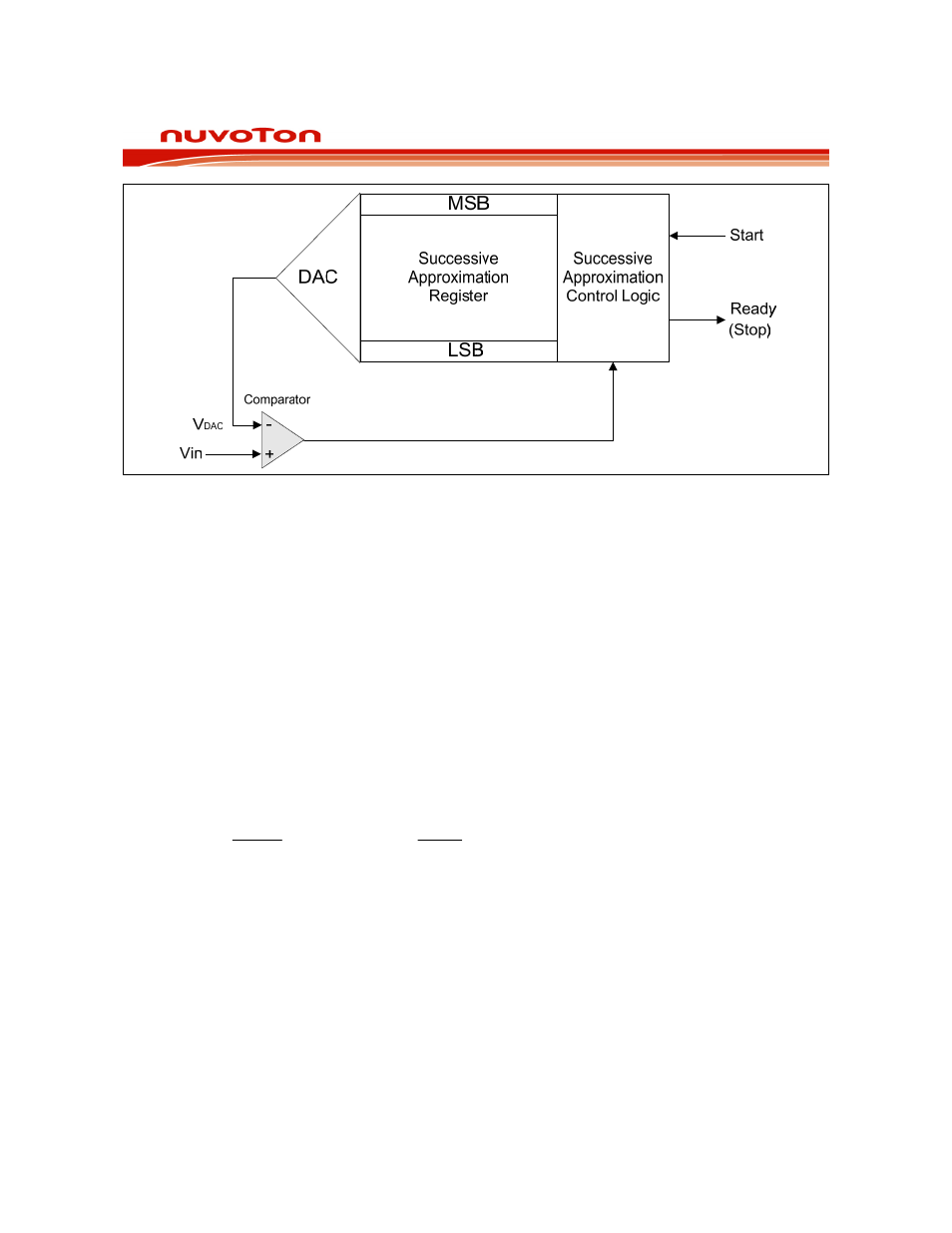
Figure 23-1: Successive Approximation ADC
23.1 ADC Resolution and Analog Supply:
The ADC circuit has its own supply pins (AVDD and AVSS) and one pins (Vref+) connected to each
end of the DAC’s resistance-ladder that the AVDD and Vref+ are connected to VDD and AVSS is
connected to VSS. The ladder has 1023 equally spaced taps, separated by a resistance of “R”. The
first tap is located 0.5×R above AVSS, and the last tap is located 0.5×R below Vref+. This gives a total
ladder resistance of 1024×R. This structure ensures that the DAC is monotonic and results in a
symmetrical quantization error.
For input voltages between VSS and [(Vref+) + ½ LSB], the 10-bit result of an A/D conversion will be
0000000000B = 000H. For input voltages between [(Vref+) – 3/2 LSB] and Vref+, the result of a
conversion will be 1111111111B = 3FFH. Vref+ and AVSS may be between AVDD + 0.2V and VSS –
0.2 V. Vref+ should be positive with respect to VSS, and the input voltage (Vin) should be between
Vref+ and VSS.
The result can always be calculated from the following formula:
Result =
Vref
Vin
1024
+
×
or Result =
VDD
Vin
1024
Ч