Rainbow Electronics W79E8213R User Manual
Page 17
Preliminary W79E8213/W79E8213R Data Sheet
Publication Release Date: July 11, 2008
- 17 -
Revision A2
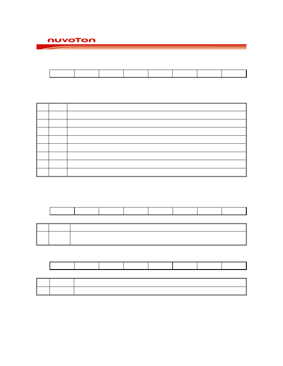
PORT 0
Bit:
7 6 5 4 3 2 1 0
P0.7 P0.6 P0.5 P0.4 P0.3 P0.2 P0.1 P0.0
Mnemonic: P0
Address: 80h
P0.7-0: General purpose Input/Output port. Most instructions will read the port pins in case of a port
read access, however in case of read-modify-write instructions, the port latch is read. These alternate
functions are described below:
BIT NAME
FUNCTION
7
P0.7
AD7 pin or Timer 1 pin by alternative.
6
P0.6
AD3 pin by alternative.
5
P0.5
AD2 pin by alternative.
4
P0.4
AD1 pin by alternative.
3
P0.3
AD0 pin by alternative.
2
P0.2
AD4 pin or BRAKE pin by alternative.
1
P0.1
AD5 pin or PWM0 pin by alternative.
0
P0.0
AD6 pin or PWM3 pin by alternative.
Note: During power-on-reset, the port pins are tri-stated. After power-on-reset, the value of the port is set by CONFIG0.PRHI
bit. The default setting for CONFIG0.PRHI =1 which the alternative function output is turned on upon reset. If
CONFIG0.PRHI is set to 0, the user has to write a 1 to port SFR to turn on the alternative function output.
STACK POINTER
Bit:
7 6 5 4 3 2 1 0
SP.7 SP.6 SP.5 SP.4 SP.3 SP.2 SP.1 SP.0
Mnemonic: SP
Address: 81h
BIT NAME
FUNCTION
7-0 SP.[7:0]
The Stack Pointer stores the Scratch-pad RAM address where the stack begins. In
other words it always points to the top of the stack.
DATA POINTER LOW
Bit:
7 6 5 4 3 2 1 0
DPL.7 DPL.6 DPL.5 DPL.4 DPL.3 DPL.2 DPL.1 DPL.0
Mnemonic: DPL
Address: 82h
BIT NAME FUNCTION
7-0
DPL.[7:0] This is the low byte of the standard 8052 16-bit data pointer.