1 working registers – Rainbow Electronics W79E8213R User Manual
Page 12
Preliminary W79E8213/W79E8213R Data Sheet
Publication Release Date: July 11, 2008
- 12 -
Revision A2
Bank 0
Bank 1
Bank 2
Bank 3
03
02
01
00
04
05
06
07
0B
0A
09
08
0C
0D
0E
0F
13
12
11
10
14
15
16
17
1B
1A
19
18
1C
1D
1E
1F
23
22
21
20
24
25
26
27
2B
2A
29
28
2C
2D
2E
2F
33
32
31
30
34
35
36
37
3B
3A
39
38
3C
3D
3E
3F
43
42
41
40
44
45
46
47
4B
4A
49
48
4C
4D
4E
4F
53
52
51
50
54
55
56
57
5B
5A
59
58
5C
5D
5E
5F
63
62
61
60
64
65
66
67
6B
6A
69
68
6C
6D
6E
6F
73
72
71
70
74
75
76
77
7B
7A
79
78
7C
7D
7E
7F
Direct RAM
Indirect RAM
00H
07H
28H
08H
0FH
10H
17H
18H
1FH
20H
21H
22H
23H
24H
25H
26H
27H
29H
2AH
2BH
2CH
2DH
2EH
2FH
30H
7FH
80H
FFH
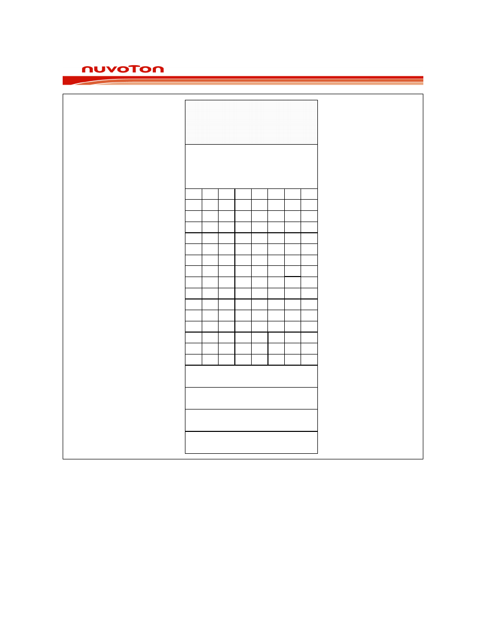
Figure 7-3: Scratch pad RAM
7.4.1 Working
Registers
There are four sets of working registers, each consisting of eight 8-bit registers. These are termed as
Banks 0, 1, 2, and 3. Individual registers within these banks can be directly accessed by separate
instructions. These individual registers are named as R0, R1, R2, R3, R4, R5, R6 and R7. However, at
one time the W79E8213 series can work with only one particular bank. The bank selection is done by
setting RS1-RS0 bits in the PSW. The R0 and R1 registers are used to store the address for indirect
accessing.