Rainbow Electronics W79E8213R User Manual
Page 27
Preliminary W79E8213/W79E8213R Data Sheet
Publication Release Date: July 11, 2008
- 27 -
Revision A2
BIT NAME
FUNCTION
7
-
Please Keep it at 0.
6~0 NVMADDR.[7:0]
The NVM address:
The register indicates NVM data memory address on On-Chip code
memory space.
TIMED ACCESS
Bit:
7 6 5 4 3 2 1 0
TA.7 TA.6 TA.5 TA.4 TA.3 TA.2 TA.1 TA.0
Mnemonic: TA
Address: C7h
BIT NAME
FUNCTION
7-0 TA.[7:0]
The Timed Access register:
The Timed Access register controls the access to protected bits. To access
protected bits, the user must first write AAH to the TA. This must be immediately
followed by a write of 55H to TA. Now a window is opened in the protected bits
for three machine cycles, during which the user can write to these bits.
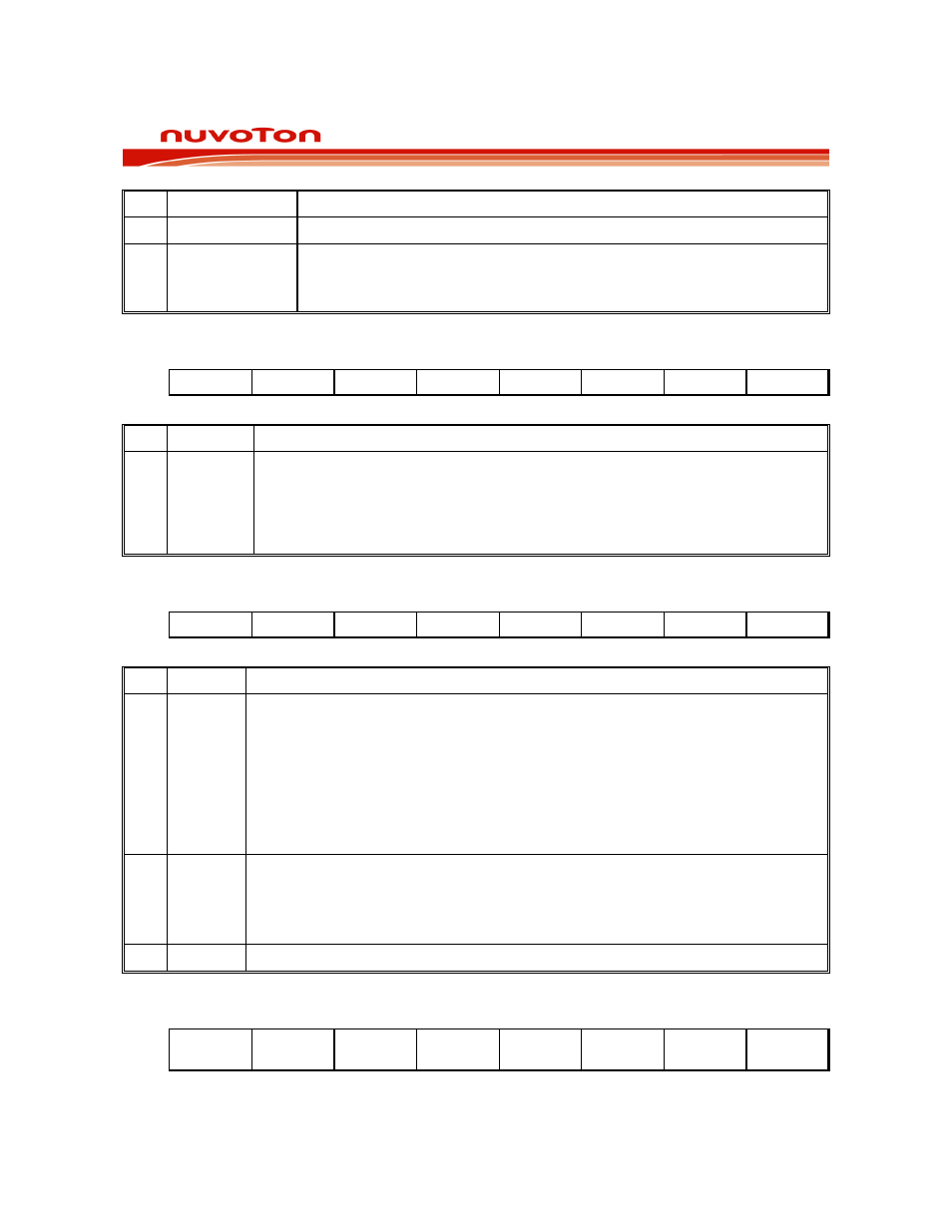
NVM CONTROL
Bit:
7 6 5 4 3 2 1 0
EER
EWR
- - - - - -
Mnemonic: NVMCON
Address: CEh
BIT NAME
FUNCTION
7 EER
NVM page(n) erase bit:
0: Without erase NVM page(n).
1: Set this bit to erase page(n) of NVM. The NVM has 8 pages and each page
have 16 bytes data memory. Initiate page select by programming NVMADDL
register, which will automaticly enable page area. When user set this bit, the
page erase process will begin and program counter will halt at this instruction.
After the erase process is completed, program counter will continue executing
next instruction.
6 EWR
NVM data write bit:
0: Without write NVM data.
1: Set this bit to write NVM bytes and program counter will halt at this instruction.
After write is finished, program counter will kept next instruction then executed.
5-0 -
Reserved
NVM DATA
Bit:
7 6 5 4 3 2 1 0
NVMDAT
A.7
NVMDAT
A.6
NVMDAT
A.5
NVMDAT
A.4
NVMDAT
A3
NVMDAT
A.2
NVMDAT
A.1
NVMDAT
A.0
Mnemonic: NVMDATA
Address: CFh