Maxq3108 low-power, dual-core microcontroller, Recommended dc operating conditions (continued) – Rainbow Electronics MAXQ3108 User Manual
Page 5
MAXQ3108
Low-Power, Dual-Core Microcontroller
_______________________________________________________________________________________
5
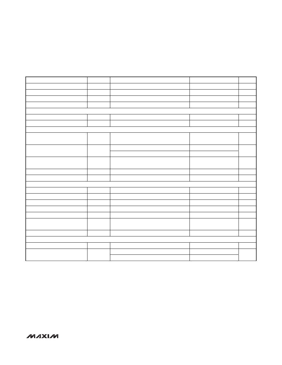
RECOMMENDED DC OPERATING CONDITIONS (continued)
(V
DD
= V
RST
to 3.6V, T
A
= -40°C to +85°C.) (Notes 1, 2)
PARAMETER SYMBOL
CONDITIONS
MIN
TYP
MAX
UNITS
Input/Output Pin Capacitance
C
IO
Guaranteed by design
15
pF
Input Low Current All Pins
I
IL
V
IN
= 0.4V
-30
μA
Input-Leakage Current
I
L
Internal pullup disabled
-100
+100
nA
Input Pullup Resistor (All Inputs)
R
PU
60 k
CLOCK SOURCE
FLL Output Frequency
f
FLL
CX1
=
32.768kHz
9.5 10.0 10.5 MHz
FLL Output Accuracy
f
FLL
CX1
=
32.768kHz
1.5
±5 %
FLASH MEMORY
System Clock During Flash
Programming/Erase
2
MHz
Mass erase
22.8
24
25.2
Flash Erase Time
Page erase
22.8
24
25.2
ms
Flash Programming Time Per
Word
(Note
7)
59.5
66.5
μs
Write/Erase
Cycles
1000 Cycles
Data Retention
T
A
= +25
°C 100
Years
SUPPLY VOLTAGE MONITOR
Set Point
SV
TR
2.0
3.5
V
Increment Resolution
0.1
V
Default Set Point
2.7
V
Current Consumption
I
SVM
10
μA
Start Time
t
SVMST
200
μs
Setup Time (Change Set Point)
t
SVM_SU1
Changing from one set point to another set
point
2
μs
Setup Time (Stop Mode Exit)
t
SVM_SU2
Exit
from
stop
mode
8
μs
REAL-TIME CLOCK
RTC Input Frequency
f
32KIN
32kHz watch crystal
32,768
Hz
V
DD
= 2.0V
0.6
RTC Operating Current
I
RTC
V
DD
= 3.6V
0.8
μA
Note 1: Results based on simulation data. Characterization data will be available at a later date. All voltages are referenced to
ground. Specifications to T
A
= -40°C are guaranteed by design and are not production tested.
Note 2: Typical values are not guaranteed. These values are measured at room temperature, V
DD
= 3.3V.
Note 3: This current is from V
BAT
only if (V
DD
< V
BAT
and V
DD
< V
RST
) or (STOP = 1, REGEN = 0, BOD = 1). Otherwise, this current
is from V
DD
.
Note 4: Measured on the V
DD
pin and the device not in reset. All inputs are connected to V
SS
or V
DD
. Outputs do not source/sink
any current. Timer enabled, RTC enabled, part executing JUMP $ from flash.
Note 5: If the RTC is on for parameters ISTOP_2, ISTOP_3, and ISTOP_4, a current equal to I
BAT1
is added to I
DD
.
Note 6: The maximum total current, I
OH(MAX)
and I
OL(MAX)
, for all outputs combined should not exceed 35mA to satisfy the maxi-
mum specified voltage drop.
Note 7: The timing listed above is clocked by 63 cycles of the internal 1MHz ±5% clock. There will be ROM code overhead, which is
a function of system clock. For data sheet purposes, a better way is to specify the limits that include ROM code execution
with specified system clock speed.