Maxq3108 low-power, dual-core microcontroller – Rainbow Electronics MAXQ3108 User Manual
Page 26
MAXQ3108
Low-Power, Dual-Core Microcontroller
26
______________________________________________________________________________________
Special Function Register Bit Descriptions (continued)
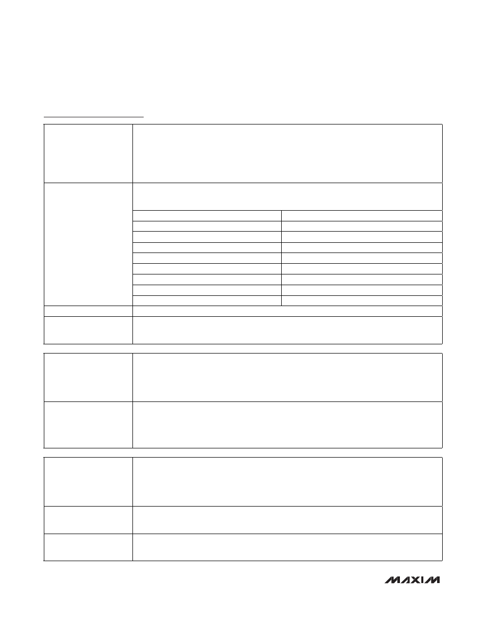
FCNTL (0Dh, 01h)
Flash Memory Control Register
Initialization:
This register is set to 80h on POR and is unaffected by all other forms of reset.
Read/Write Access:
Unrestricted read, bits 2:0 are write accessible only by utility ROM or logical data memory. (This
register is not accessible by program code inside the flash memory because of the rule governing
the pseudo-Von Neumann mapping. Access is blocked by hardware.) Also, write access to FCNTL
is prohibited when FBUSY is 0.
Flash Command Bits 2:0. The below table shows the commands for flash operations provided by
these bits. The MMU supports only these commands; other settings are reserved. Using any
reserved command results in no operation.
FC[2:0] FLASH
COMMANDS
000
Read Mode (default)
001
Verify Information Block
010 Write
Information
Block
011
Write Main Memory Block
100
Erase Information Block
101
Page Erase of Main Memory Block
110
Mass Erase of Main Memory Block
FCNTL.[2:0]: FC[2:0]
111
Load Trim Information
FCNTL.[6:3]: Reserved
Reserved. Reads return 0.
FCNTL.7: FBUSY
Flash Busy. This busy flag is cleared to a logic 0 to indicate the start of an erase/program
operation by the MMU immediately following the command sequence. It is hold low until the end of
the operation. Set/reset of this flag is synchronized with the system clock.
FDATA (0Eh, 01h)
Flash Memory Data Register
Initialization:
This register is cleared to 0000h on all forms of reset.
Read/Write Access:
Unrestricted read, write accessible only by utility ROM or logical data memory. (This register is not
accessible for program code inside the flash memory due to the rule governing the pseudo-Von
Neumann mapping.). Also, write access to FCNTL is prohibited when FBUSY is 0.
FDATA.[15:0]:
This register is used by the user software or the ROM loader to support the flash
erase/program/verify operation. Writing to this SFR has no effect on flash operation until a valid
flash command is first entered through the FC[2:0] bits of the FCNTL SFR. All flash operation must
be initiated by providing a valid command in the FCNTL control register followed by writing target
address and data by the FDATA SFR (when required by the command).
PWCN (0Fh, 01h)
Power Control Register (16-Bit Register)
Initialization:
Implemented register bits (except for the ECLKO and ENDSP bit) are unaffected by resets other than
power-on reset. The ECLKO and ENDSP bits are reset to 0 on any reset. On power-on reset, this
register is reset to 0000h (except that HFXD is 1 for PCK = 11b).
Read/Write Access:
Unrestricted read. FLOCK and 32KRDY are read-only.
PWCN.0: FLLEN
FLL Lock Enable. Setting this bit to 1 enables the FLL if it is not already running, and causes it to
lock to the 32K input. When this bit is cleared to 0, the FLL is disabled if it is not providing the
system clock.
PWCN.1: FLOCK
FLL Locked. This is a read-only status bit. This bit is automatically reset to 0 when FLLEN is
changed from 0 to 1 and set to 1 when the FLL is locked to the 32.768kHz clock. This bit is also
reset to 0 on entry to stop mode.