Peripheral registers—dspcore, Table 3. dspcore peripheral registers, Maxq3108 low-power, dual-core microcontroller – Rainbow Electronics MAXQ3108 User Manual
Page 15
MAXQ3108
Low-Power, Dual-Core Microcontroller
______________________________________________________________________________________
15
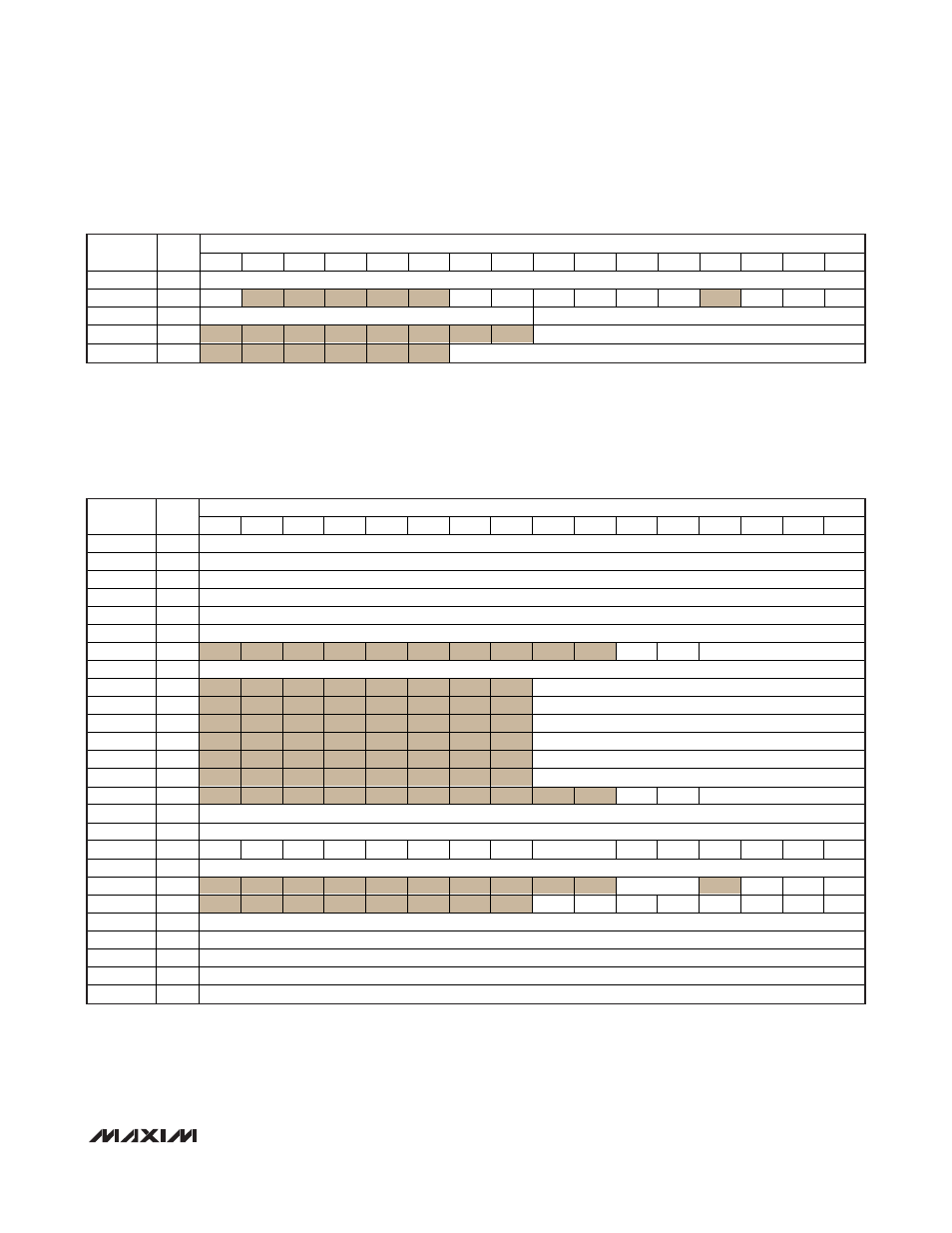
Peripheral Registers—DSPCore
The MAXQ3108 DSPCore exposes its peripheral com-
plement in modules numbered 0 and 1. Table 3
describes the functions associated with the peripheral
registers, and Table 4 shows the default values of these
registers.
BIT
REGISTER
MOD:
REG
15
14
13
12
11
10 9 8 7 6 5 4 3 2 1 0
TB0V 4:11
0x0000
I2CCN 4:12 0
0 0 0 0 0 0 0 0 0
I2CCK 4:13
0x02
0x04
I2CTO 4:14
0x00
I2CSLA 4:15
0x000
Table 2. UserCore Peripheral Register Default Values (continued)
BIT
REGISTER
MOD:
REG
15
14
13
12
11
10 9 8 7 6 5 4 3 2 1 0
AD0 0:0
ADC0
Output
Register
AD1 0:1
ADC1
Output
Register
AD2 0:2
ADC2
Output
Register
AD3 0:3
ADC3
Output
Register
AD4 0:4
ADC4
Output
Register
AD5 0:5
ADC5
Output
Register
SRSP0 0:6
RSPSDV
REQE RSPST
SRSP1
0:7
Slave Response Register 1
AD0LSB 0:8
ADC0 Output Register LSB
AD1LSB 0:9
ADC1 Output Register LSB
AD2LSB 0:10
ADC2 Output Register LSB
AD3LSB 0:11
ADC3 Output Register LSB
AD4LSB 0:12
ADC4 Output Register LSB
AD5LSB 0:13
ADC5 Output Register LSB
MREQ0 0:14
REQCDV
RSPIE REQCM
MREQ1
0:15
Master Request Register 1
MREQ2
0:16
Master Request Register 2
ADCN 0:17
IFCSEL
IF45E
IF23E
IF10E
MD CKS
MD2E MD1E MD0E
OSRI
ABF5 ABF4 ABF3 ABF2 ABF1 ABF0
ADCC
0:18
ADC Clock Correction Register
MSTC 0:19
CCSL
MD2SNC MD1SNC MD0SNC
MCNT 1:0
OF
MCW
CLD
SQU
OPCS
MSUB
MMAC
SUS
MA 1:1
Multiplier
Operand
“A”
Register
MB 1:2
Multiplier
Operand
“B”
Register
MC2
1:3
Multiplier Accumulator Register 2 (MSB, bits 47-32)
MC1
1:4
Multiplier Accumulator Register 1 (bits 31-16)
MC0
1:5
Multiplier Accumulator Register 0 (LSB, bits 15-0)
Table 3. DSPCore Peripheral Registers