Maxq3108 low-power, dual-core microcontroller – Rainbow Electronics MAXQ3108 User Manual
Page 18
MAXQ3108
Low-Power, Dual-Core Microcontroller
18
______________________________________________________________________________________
Special Function Register Bit Descriptions (continued)
SRSP1 (07h, 00h)
Slave Response Register 1
Initialization:
This register is reset to 0000h on all forms of reset.
Read/Write Access:
Unrestricted read access only to the UserCore.
Unrestricted read/write access to the DSPCore.
SRSP1.[15:0]:
Response Register 1 Bits 15:0. These bits are used to supply output data to the master. To notify
the master that data is ready to be read, the RSPCDV bit should be set to 1 by software. The slave
should not write further data to SRSP1 until the valid condition (RSPSDV = 1) is cleared by the
master software.
AD0LSB (08h, 00h)
Analog-to-Digital Converter 0 Least Significant Byte Output Register
Initialization:
This register is reset to FFh on all forms of reset.
Read/Write Access:
Unrestricted read access.
Analog-to-Digital Converter 0 Least Significant Byte Output Register. This register always provides
read access to the least significant byte of the most current ADC0 data sample acquired from the
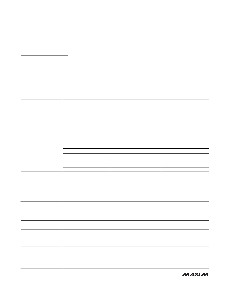
respective sinc3 filter. See the below table for the least significant byte available OSR options.
Reading from the AD0 register results in the ABF0 flag being cleared by hardware (when set)
unless the read operation is performed simultaneously with a write. What this means is that when
OSR > 32, AD0LSB should be read first if the clearing of ABF0 is intended to indicate that the full
result (AD0LSB and AD0) was read. Reading a disabled ADC returns the data last acquired if the
associated buffer full flag is set and returns FFFFh if the flag is clear.
OSR
ADC DATA OUTPUT WIDTH
AD0LSB FORMAT
32 16
00000000b
64 19
d2–d0,
00000b
128 22
d5–d0,
00b
AD0LSB.[7:0]:
256 24
d7–d0
AD1LSB (09h, 00h)
Analog-to-Digital Converter 1 Least Significant Byte Output Register
AD2LSB (0Ah, 00h)
Analog-to-Digital Converter 2 Least Significant Byte Output Register
AD3LSB (0Bh, 00h)
Analog-to-Digital Converter 3 Least Significant Byte Output Register
AD4LSB (0Ch, 00h)
Analog-to-Digital Converter 4 Least Significant Byte Output Register
AD5LSB (0Dh, 00h)
Analog-to-Digital Converter 5 Least Significant Byte Output Register
MREQ0 (0Eh, 00h)
Master Request Register 0
Initialization:
This register is reset to 00h on all forms of reset.
Read/Write Access:
Unrestricted read/write access to the UserCore (except REQCDV; see the bit description).
Unrestricted read access only to the DSPCore (except REQCDV; see the bit description).
MREQ0.[3:0]: REQCM[3:0]
Request Command Bits 3:0. These bits are written by the master to supply a command request to the
slave. To notify the slave that a command is ready to be read, the REQ0DV bit should be set to 1.
MREQ0.4: RSP1E
Response Registers Interrupt Enable. Setting this bit to 1 enables an interrupt for the slave
response status data valid flag (which is associated with Response Registers 0 and 1). The status
data valid (interrupt) flag is reported in SRSP0.5. Clearing this bit to 0 disables the interrupt
associated with the response status data valid flag.
MREQ0.5: REQCDV
Request Command Data Valid Flag. This flag can only be set by the master (UserCore). This flag
should be set once a valid command is supplied in the REQCM[3:0] field of the MREQ0 and/or data
supplied in the MREQ1, MREQ2 registers to notify the slave that these registers are ready for
reading. This flag can only be cleared by slave (DSPCore) software.
MREQ0.[7:6]: Reserved
Reserved. Reads return 0.