Absolute maximum ratings, Recommended dc operating conditions, Maxq3108 low-power, dual-core microcontroller – Rainbow Electronics MAXQ3108 User Manual
Page 4
MAXQ3108
Low-Power, Dual-Core Microcontroller
4
_______________________________________________________________________________________
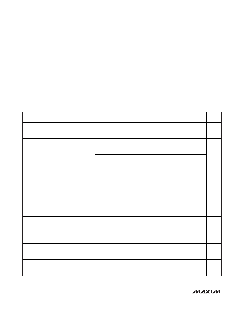
RECOMMENDED DC OPERATING CONDITIONS
(V
DD
= V
RST
to 3.6V, T
A
= -40°C to +85°C.) (Notes 1, 2)
Stresses beyond those listed under “Absolute Maximum Ratings” may cause permanent damage to the device. These are stress ratings only, and functional
operation of the device at these or any other conditions beyond those indicated in the operational sections of the specifications is not implied. Exposure to
absolute maximum rating conditions for extended periods may affect device reliability.
Voltage Range on Any Pin
except V
DD
with Respect to V
SS
...........................-0.3V to V
DD
Voltage Range on V
DD
with Respect to V
SS
.........-0.3V to +3.6V
Operating Temperature Range ...........................-40°C to +85°C
Storage Temperature Range .............................-65°C to +150°C
Soldering Temperature...........................Refer to the IPC/JEDEC
J-STD-020 Specification.
PARAMETER SYMBOL
CONDITIONS
MIN
TYP
MAX
UNITS
Supply Voltage
V
DD
V
RST
3.6 V
Power-Fail Reset Voltage
V
RST
Monitors
V
DD
1.875 1.975 V
1.8V Internal Regulator
V
REG18
1.71 1.8 1.89 V
1.8V Power-Fail Reset Voltage
V
REGRST
Monitors
REGOUT
1.62
1.71
V
Battery Supply Voltage
V
BAT
1.8
3.6
V
V
DD
= 0, V
BAT
= 3.6V, 32kHz oscillator and
RTC enabled
0.8
Battery Current (Note 3)
I
BAT1
V
DD
= 0, V
BAT
= 2V, 32kHz oscillator and
RTC enabled
0.6
μA
I
DD_FLL1
/1
mode,
V
DD
= 2.0V
1.3
2.2
I
DD_FLL2
/1
mode,
V
DD
= 3.6V
1.5
2.5
I
DD_FLL9
PMM2 (32kHz), V
DD
= 2.0V
0.5
0.8
Active Current with 32.768kHz
Crystal Connected to CX1, CX2;
FLL Selected (10MHz Output);
ENDSP = 0; All Decimators and
Sinc Filters Off (Note 4)
I
DD_FLL10
PMM2 (32kHz), V
DD
= 3.6V
0.6
1.0
mA
I
DD_FLL14
V
DD
= 2.0V
1.0
1.7
Active Current with 32.768kHz
Crystal Connected to CX1, CX2;
FLL Selected (10MHz Output);
UserCore = /256 PMM; DSPCore
= /1 ; ENDSP = 1; Manchester
Decoders On; Decimators On
I
DD_FLL15
V
DD
= 3.6V
1.8
3.0
mA
I
STOP_1
BOD = 1, REGEN = 0, SVMSTOP = 0, RTC
off (lowest current stop mode)
0.1
2.4
Stop-Mode Current (Note 5)
I
STOP_2
BOD = 0, REGEN = 0, SVMSTOP = 0, RTC
off (adds brownout-reset detection)
30
125
μA
Input Low (CX1)
V
IL1
V
SS
0.20
x
V
DD
V
Input Low (All Other Pins)
V
IL2
V
SS
0.30
x
V
DD
V
Input High (CX1)
V
IH1
0.75
x
V
DD
V
DD
V
Input High (All Other Pins)
V
IH2
0.70
x
V
DD
V
DD
V
Input Hysteresis (Schmitt)
V
IHYS
0.18
V
Output Low (All Port Pins)
V
OL
I
OL
= 4mA (Note 6)
V
SS
0.4 V
Output High (All Port Pins)
V
OH
I
OH
= -4mA (Note 6)
V
DD
- 0.4
V
ABSOLUTE MAXIMUM RATINGS