Maxq3108 low-power, dual-core microcontroller – Rainbow Electronics MAXQ3108 User Manual
Page 33
MAXQ3108
Low-Power, Dual-Core Microcontroller
______________________________________________________________________________________
33
Special Function Register Bit Descriptions (continued)
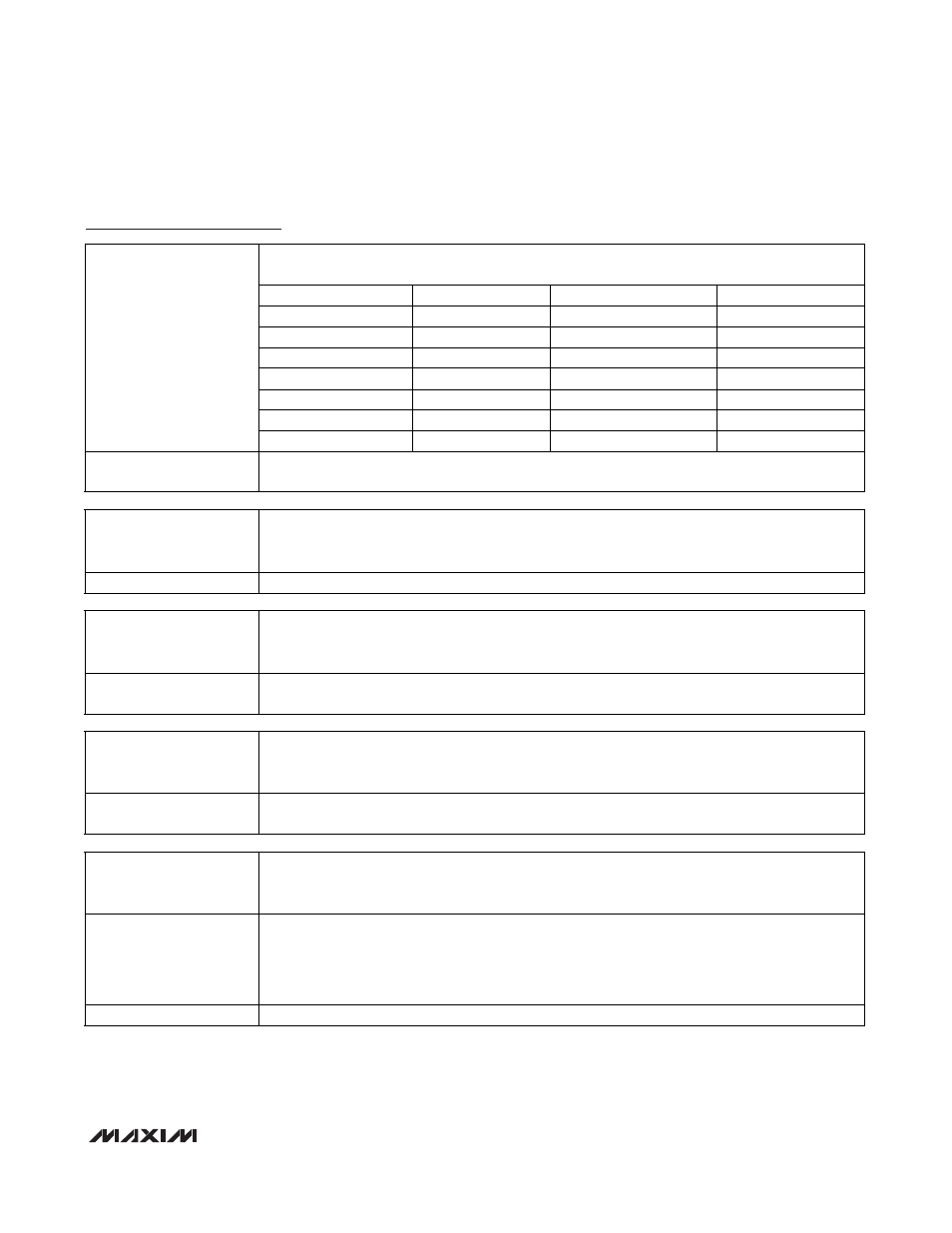
Timer 2 Output Enable 0. This register bit enables the timer 2 output function for the external T2P
pin. The table below shows timer 2 output possibilities for the T2, T2PB pins.
T20E[1:0]
T2MD
T2P PIN
T2PB PIN
00
X
Port latch data
Port latch data
01
0
16-bit PWM output
Port latch data
10
0
Port latch data
16-bit PWM output
11
0
16-bit PWM output
16-bit PWM output
01
1
8-bit PWM output (T2H)
Port latch data
10
1
Port latch data
8-bit PWM output (T2L)
T2CNA.6: T2OE0
11
1
8-bit PWM output (T2H)
8-bit PWM output (T2L)
T2CNA.7: ET2
Enable Timer 2 Interrupts. This bit serves as the local enable for timer 2 interrupt sources that fall
under the TF2 and TCC2 interrupt flags.
T2H (01h, 02h)
Timer 2 Most Significant Byte
Initialization:
The timer 2 most significant byte is cleared to 00h on all forms of reset.
Read/Write Access:
Unrestricted read/write.
T2H.[7:0]:
Timer 2 MSB Bits 7:0. This register is used to load and read the most significant 8-bit value in timer 2.
T2RH (02h, 02h)
Timer 2 Most Significant Byte Reload
Initialization:
The timer 2 most significant byte is cleared to 00h on all forms of reset.
Read/Write Access:
Unrestricted read/write.
T2RH.[7:0]:
Timer 2 Reload MSB Bits 7:0. This register is used to load and read the most significant 8-bit
value in timer 2.
T2CH (03h, 02h)
Timer 2 Most Significant Byte Capture/Compare
Initialization:
This byte is cleared to 00h on all forms of reset.
Read/Write Access: Unrestricted
read/write.
T2CH.[7:0]:
Timer 2 Capture/Compare MSB Bits 7:0. This register reflects the upper byte of the timer 2
capture/compare value and is read/write accessible at all times.
PO2 (04h, 02h)
Port 2 Output Register (8-Bit Register)
Initialization:
This register is set to 1Fh on all forms of reset.
Read/Write Access: Unrestricted
read/write.
PO2.[6:0]:
Port 2 Output Register Bits 6:0. The PO2 register stores output data for port 2 when it is defined as
an output port and controls whether the internal weak p-channel pullup transistor is
enabled/disabled if a port pin is defined as an input. The contents of this register can be modified
by a write access. Reading from the register returns the contents of the register. Changing the
direction of port 2 does not change the data contents of the register.
PO2.7: Reserved
Reserved. Reads return 0.