Dsp program ram, Registers, System registers – Rainbow Electronics MAXQ3108 User Manual
Page 10: Peripheral registers—usercore, Table 1. usercore peripheral registers, Maxq3108 low-power, dual-core microcontroller
MAXQ3108
Low-Power, Dual-Core Microcontroller
10
______________________________________________________________________________________
DSP Program RAM
A 4K Word (8KB) section of memory is available to the
DSPCore as code memory. When the DSPCore is dis-
abled (as it is immediately following a reset event) that
block of memory appears in the UserCore data memory
map at location 0x1000. Thus, a typical startup
sequence to operate both cores might include:
1) Low-level initialization of the UserCore.
2) Copy DSP code from program flash to DSPCore
code RAM at 0x1000.
3) Enable DSPCore.
4) Poll mailbox registers to verify that DSPCore is cor-
rectly running.
For more information, see the
Dual-Core Interfaces
section.
Registers
The MAXQ family of microcontrollers uses a bank of
registers to access memory and peripherals and to per-
form basic CPU activities. These registers are orga-
nized into as many as 16 register modules, each of
which can have as many as 32 registers, giving a sys-
tem maximum of 512 registers. The registers are divid-
ed into two sections: system registers (modules 7 to 15)
and peripheral registers (modules 0 to 5).
Since the MAXQ3108 contains two MAXQ core proces-
sors, each has a set of system registers and a set of
peripheral registers.
System Registers
The MAXQ3108 UserCore implements the standard set
of system registers as described in the
MAXQ Family
User’s Guide
. The exceptions are listed below:
• In the IMR register, bit IM5 is not implemented since
there is no module 5 implemented in the MAXQ3108.
• In the SC register, bits CDA1 and UPM are not imple-
mented since the size of the memory in the device
does not require their implementation.
• In the IIR register, bit II5 is not implemented since
there is no module 5 implemented in the MAXQ3108.
• In the CKCN register, bits XT/RC, RGSL, and
RGMD are not implemented. Instead, bits 5 and 6
are FLLMD and FLLSL, respectively. These bits
support the frequency-locked loop (FLL) that forms
a core part of the MAXQ3108 clocking scheme.
More information is given in the
Clock
section.
The MAXQ3108 DSPCore system register complement
is identical to that found in the UserCore, with these
exceptions:
• In the IMR register, only IM0 is implemented.
• The system control (SC) register is not implemented.
• In the IIR register, only the II0 bit is implemented.
• The WDCN register is not implemented because
there is no watchdog timer in the DSPCore.
Watchdog functionality can be implemented in the
UserCore by determining if the DSPCore is respond-
ing to messages.
• In the CKCN register, the STOP, RGSL, and SWB bits
are not implemented because the corresponding
functions do not exist in the DSPCore. The FLLMD
and FLLSL bits are not implemented because a com-
mon clock block is shared with the UserCore, and
the control bits here would be redundant.
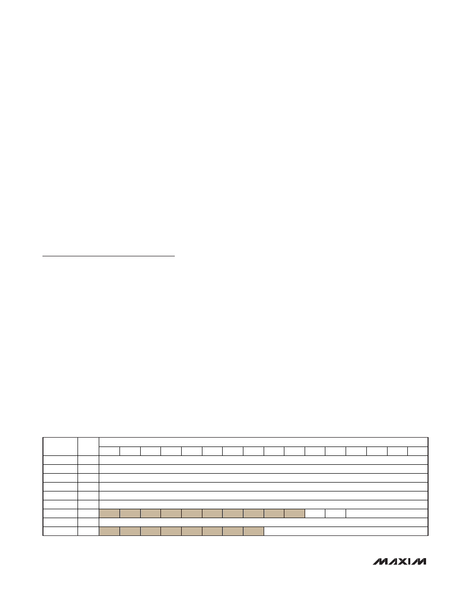
Peripheral Registers—UserCore
The MAXQ3108 UserCore exposes its peripheral com-
plement in five modules numbered 0 to 4. Table 1
describes the functions associated with the peripheral
registers, and Table 2 shows the default values of these
registers.
BIT
REGISTER
MOD:
REG
15
14
13
12
11
10 9 8 7 6 5 4 3 2 1 0
AD0 0:0
ADC0
Output
Register
AD1 0:1
ADC1
Output
Register
AD2 0:2
ADC2
Output
Register
AD3 0:3
ADC3
Output
Register
AD4 0:4
ADC4
Output
Register
AD5 0:5
ADC5
Output
Register
SRSP0 0:6
RSPSDV
REQE RSPST
SRSP1
0:7
Slave Response Register 1
AD0LSB 0:8
ADC0 Output Register LSB
Table 1. UserCore Peripheral Registers