4 switching characteristics for pci interface, 5 switching characteristics for phy-link interface – Texas Instruments TSB12LV26 User Manual
Page 87
7–3
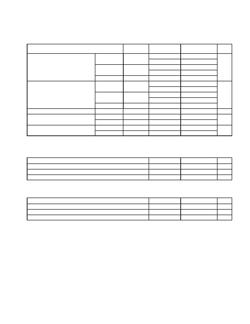
7.3
Electrical Characteristics Over Recommended Operating Conditions (unless
otherwise noted)
OPERATION
TEST
CONDITIONS
MIN
MAX
UNIT
PCI
IOH = – 0.5 mA
0.9 VCC
PCI
IOH = – 2 mA
2.4
VOH
High-level output voltage
PHY interface
IOH = – 4
µ
A
2.8
V
PHY interface
IOH = – 8 mA
VCC – 0.6
Miscellaneous‡
IOH = – 4 mA
VCC – 0.6
†
PCI
IOL = 1.5 mA
0.1 VCC
†
PCI
IOL = 6 mA
0
0.55
VOL†
Low-level output voltage
PHY interface
IOL = 4 mA
0.4
V
PHY interface
IOL = 8 mA
Miscellaneous‡
IOL = 4 mA
0.5
IOZ
3-state output high-impedance
Output pins
3.6 V
VO = VCC or GND
±
20
µ
A
IIL
Low level input current
Input pins
3.6 V
VI = GND‡
±
20
µ
A
IIL
Low-level input current
I/O pins†
3.6 V
VI = GND‡
±
20
µ
A
IIH
High level input current
PCI†
3.6 V
VI = VCC‡
±
20
µ
A
IIH
High-level input current
Others†
3.6 V
VI = VCC‡
±
20
µ
A
† For I/O pins, input leakage (IIL and IIH) includes IOZ of the disabled output.
‡ Miscellaneous pins are: GPIO2, GPIO3, SDA, SCL, CYCLEOUT.
7.4
Switching Characteristics for PCI Interface
§
PARAMETER
MEASURED
MIN
TYP
MAX
UNIT
tsu
Setup time before PCLK
–50% to 50%
3
ns
th
Hold time before PCLK
–50% to 50%
0
ns
td
Delay time, PHY_CLK to data valid
–50% to 50%
2
6
ns
§ These parameters are ensured by design.
7.5
Switching Characteristics for PHY-Link Interface
§
PARAMETER
MEASURED
MIN
TYP
MAX
UNIT
tsu
Setup time, Dn, CTLn, LREQ to PHY_CLK
–50% to 50%
6
ns
th
Hold time, Dn, CTLn, LREQ before PHY_CLK
–50% to 50%
1
ns
td
Delay time, PHY_CLK to Dn, CTLn
–50% to 50%
2
11
ns
§ These parameters are ensured by design.