Texas Instruments TSB12LV26 User Manual
Page 21
3–1
3 TSB12LV26 Controller Programming Model
This section describes the internal registers used to program the TSB12LV26. All registers are detailed in the same
format: a brief description for each register, followed by the register offset and a bit table describing the reset state
for each register.
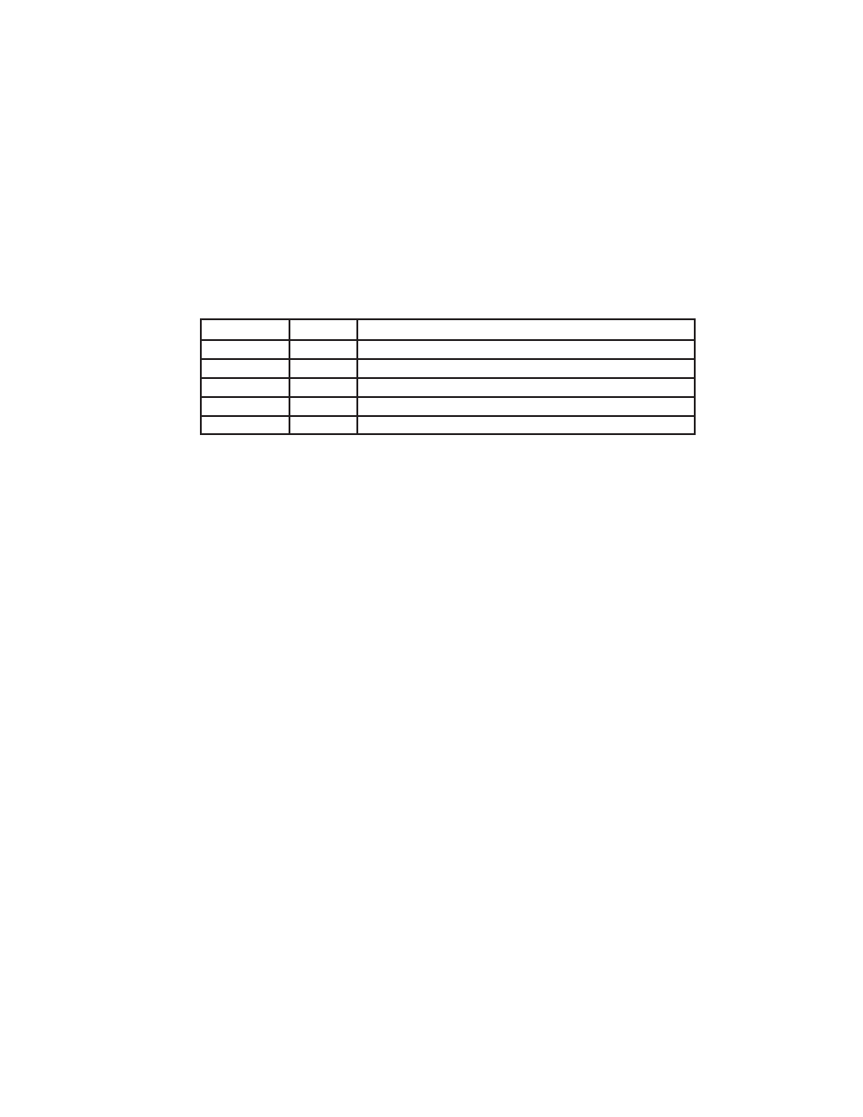
A bit description table, typically included when the register contains bits of more than one type or purpose, indicates
bit field names, field access tags which appear in the
type column,and a detailed field description. Table 3–1
describes the field access tags.
Table 3–1. Bit Field Access Tag Descriptions
ACCESS TAG
NAME
MEANING
R
Read
Field may be read by software.
W
Write
Field may be written by software to any value.
S
Set
Field may be set by a write of 1. Writes of 0 have no effect.
C
Clear
Field may be cleared by a write of 1. Writes of 0 have no effect.
U
Update
Field may be autonomously updated by the TSB12LV26.
A simplified block diagram of the TSB12LV26 is provided in Figure 3–1.