2 terminal descriptions – Texas Instruments TSB12LV26 User Manual
Page 13
2–1
2 Terminal Descriptions
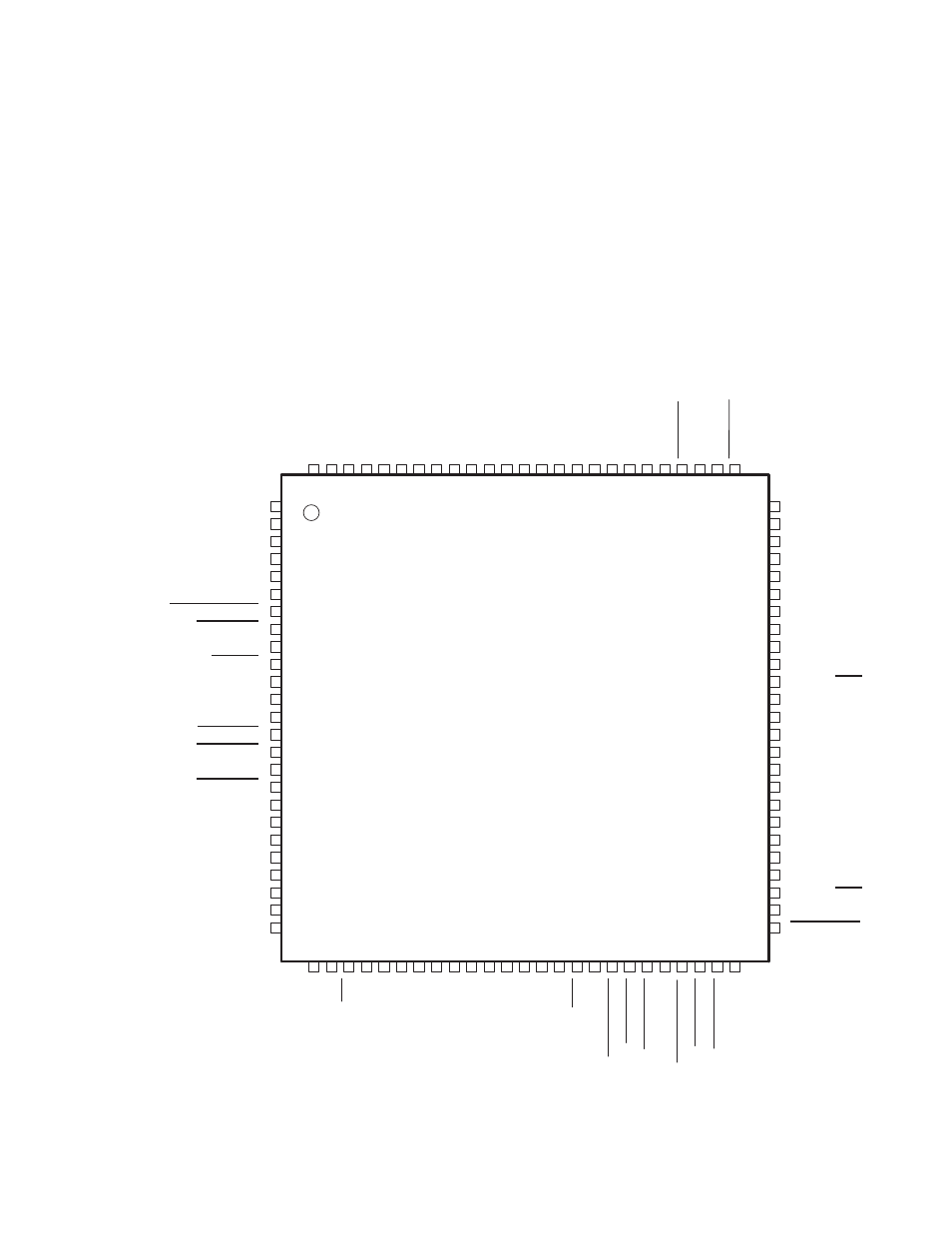
This section provides the terminal descriptions for the TSB12LV26. Figure 2–1 shows the signal assigned to each
terminal in the package. Table 2–1 is a listing of signal names arranged in terminal number order, and Table 2–2 lists
terminals in alphanumeric order by signal names.
1
2
3
4
5
6
7
8
9
10
11
12
13
14
15
16
17
18
19
20
21
22
23
24
25
76
77
78
79
80
81
82
83
84
85
86
87
88
89
90
91
92
93
94
95
96
97
98
99
100
75
74
73
72
71
70
69
68
67
66
65
64
63
62
61
60
59
58
57
56
55
54
53
52
51
50
49
48
47
46
45
44
43
42
41
40
39
38
37
36
35
34
33
32
31
30
29
28
27
26
REG18
PHY_SCLK
GND
PHY_DA
T
A
1
PHY_DA
T
A
2
PHY_DA
T
A
5
GND
PHY_DA
T
A
6
PHY_DA
T
A
7
PCI_AD25
PCI_AD24
PCI_C/BE3
PCI_IDSEL
GND
PCI_AD18
PCI_AD17
PCI_AD16
GND
REG18
PZ PACKAGE
(TOP VIEW)
PHY_DA
T
A
0
PCI_AD21
PHY_LREQ
PHY_DA
T
A
3
PHY_DA
T
A
4
PCI_AD19
GPIO2
GPIO3
SCL
SDA
V
CCP
PCI_CLKRUN
PCI_INTA
3.3 V
CC
G_RST
GND
PCI_CLK
PCI_GNT
V
CCP
PCI_AD30
3.3 V
CC
PCI_AD29
PCI_AD28
PCI_AD27
GND
PCI_AD26
3.3 V
CC
PCI_REQ
PCI_PME
PCI_AD31
GND
GND
PCI_AD1
PCI_AD2
3.3 V
CC
PCI_AD5
PCI_AD7
PCI_AD8
PCI_AD9
GND
PCI_AD12
PCI_AD14
PCI_AD15
PCI_C/BE1
PCI_AD0
PCI_AD3
PCI_AD4
PCI_AD6
PCI_C/BE0
V
CCP
PCI_AD10
PCI_AD11
PCI_AD13
3.3 V
CC
PCI_PAR
PCI_SERR
PCI_RST
CYCLEOUT
CYCLEIN
REG_EN
CCP
V
CC
3.3 V
PHY_CTL1
PHY_CTL0
CC
3.3 V
PHY_LINKON
PHY_LPS
PCI_AD22
PCI_AD23
PCI_AD20
CCP
V
PCI_C/BE2
PCI_FRAME
PCI_IRDY
PCI_TRDY
PCI_DEVSEL
PCI_ST
OP
PCI_PERR
CC
3.3 V
CC
3.3 V
CC
3.3 V
Figure 2–1. Terminal Assignments