Texas Instruments TSB12LV26 User Manual
Page 16
2–4
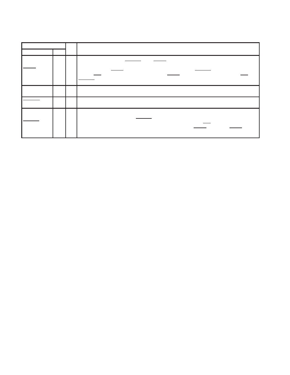
Table 2–4. PCI System Terminals
TERMINAL
I/O
DESCRIPTION
NAME
NO.
I/O
DESCRIPTION
G_RST
10
I
Global power reset. This reset brings all of the TSB12LV26 internal registers to their default states, including
those registers not reset by PCI_RST. When G_RST is asserted, the device is completely nonfunctional.
When implementing wake capabilities from the 1394 host controller, it is necessary to implement two resets
to the TSB12LV26. G_RST should be a one-time power-on reset, and PCI_RST should be connected to the
PCI bus RST. If wake capabilities are not required, G_RST may be connected to the PCI bus RST (see
PCI_RST, terminal 76).
PCI_CLK
12
I
PCI bus clock. Provides timing for all transactions on the PCI bus. All PCI signals are sampled at rising edge
of PCI_CLK.
PCI_INTA
8
O
Interrupt signal. This output indicates interrupts from the TSB12LV26 to the host. This terminal is implemented
as open-drain.
PCI_RST
76
I
PCI reset. When this bus reset is asserted, the TSB12LV26 places all output buffers in a high impedance state
and resets all internal registers except device power management context- and vendor-specific bits initialized
by host power-on software. When PCI_RST is asserted, the device is completely nonfunctional.
If this terminal is implemented, then it should be connected to the PCI bus RST signal. Otherwise, it should
be pulled high to link VCC through a 4.7-k
Ω
resistor, or strapped to the G_RST terminal (see G_RST, terminal
10).