30 phy layer control register – Texas Instruments TSB12LV26 User Manual
Page 64
4–26
4.30 PHY Layer Control Register
The PHY layer control register is used to read or write a PHY register. See Table 4–21 for a complete description of
the register contents.
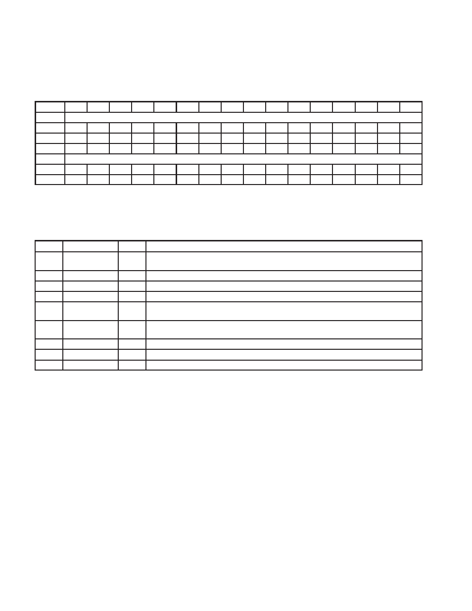
Bit
31
30
29
28
27
26
25
24
23
22
21
20
19
18
17
16
Name
PHY layer control
Type
RU
R
R
R
RU
RU
RU
RU
RU
RU
RU
RU
RU
RU
RU
RU
Default
0
0
0
0
0
0
0
0
0
0
0
0
0
0
0
0
Bit
15
14
13
12
11
10
9
8
7
6
5
4
3
2
1
0
Name
PHY layer control
Type
RWU
RWU
R
R
R/W
R/W
R/W
R/W
R/W
R/W
R/W
R/W
R/W
R/W
R/W
R/W
Default
0
0
0
0
0
0
0
0
0
0
0
0
0
0
0
0
Register:
PHY layer control
Type:
Read/Write/Update, Read/Write, Read/Update, Read-only
Offset:
ECh
Default:
0000 0000h
Table 4–21. PHY Control Register Description
BIT
FIELD NAME
TYPE
DESCRIPTION
31
rdDone
RU
This bit is cleared to 0 by the TSB12LV26 when either bit 15 (rdReg) or bit 14 (wrReg) is set. This bit is
set when a register transfer is received from the PHY.
30–28
RSVD
R
Reserved. Bits 30–28 return 0s when read.
27–24
rdAddr
RU
This is the address of the register most recently received from the PHY.
23–16
rdData
RU
This field is the contents of a PHY register which has been read.
15
rdReg
RWU
This bit is set by software to initiate a read request to a PHY register and is cleared by hardware when
the request has been sent. Bits 14 (wrReg) and 15 (rdReg) must be used exclusively.
14
wrReg
RWU
This bit is set by software to initiate a write request to a PHY register and is cleared by hardware when
the request has been sent. Bits 14 (wrReg) and 15 (rdReg) must be used exclusively.
13–12
RSVD
R
Reserved. Bits 13–12 return 0s when read.
11–8
regAddr
R/W
This field is the address of the PHY register to be written or read.
7–0
wrData
R/W
This field is the data to be written to a PHY register and is ignored for reads.