Development board block diagram, Handling the board – Altera Cyclone V SoC Development Board User Manual
Page 8
1–4
Chapter 1: Overview
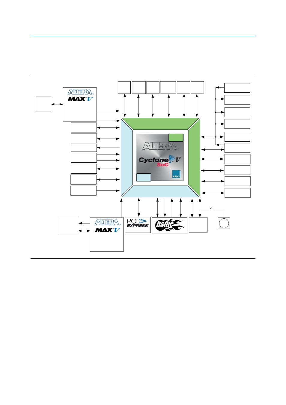
Development Board Block Diagram
Cyclone V SoC Development Board
November 2013
Altera Corporation
Reference Manual
Development Board Block Diagram
shows a block diagram of the Cyclone V SoC development board.
Handling the Board
When handling the board, it is important to observe the following static discharge
precaution:
c
Without proper anti-static handling, the board can be damaged. Therefore, use
anti-static handling precautions when touching the board.
Figure 1–1. Cyclone V SoC Development Board Block Diagram
JTAG Chain
LEDs
DIP
Switches
Push
Buttons
LVDS/Single-Ended
x4
x40
x40
x40
x4
x4
x4
x16
ADDR
XCVR x4
XCVR x4
XCVR x4
x40
x8
CLKIN x3
CLKOUT x3
x8 CONFIG
x4
x4
I
2
C
x1
x1
x1
x1
x8
x4
x4
x8
x1
x1
x19 Blaster
Accelerator Bus
USB 2.0
OTG
UART
CAN
LCD Character
64-MB QSPI
Flash
SD Card
Socket
SPI + I
2
C LTC
Exp Header
EEPROM
Real-Time
Clock
LTC Power I
2
C
Header
LTC Power
Monitor
1024 MB
DDR3 + ECC
1024 MB
DDR3 + ECC
Push Buttons +
DIP Switches
50 MHz /100 MHz
Fixed Oscillator
10/100
Ethernet
10/100
EtherCAT
REFCLK
VCXO
LEDs
EPM570GM100
Embedded
USB-Blaster II
and USB Interface
Mini-USB
2.0
128-MB
NOR
Flash
SDI
x1
SMA
5M2210ZF256I5N
System Controller
x4
Gigabit
Ethernet PHY
5CSXFC6D6F31C7
FPGA
HPS