Altera Cyclone V SoC Development Board User Manual
Page 17
Chapter 2: Board Components
2–9
MAX V CPLD 5M2210 System Controller
November 2013
Altera Corporation
Cyclone V SoC Development Board
Reference Manual
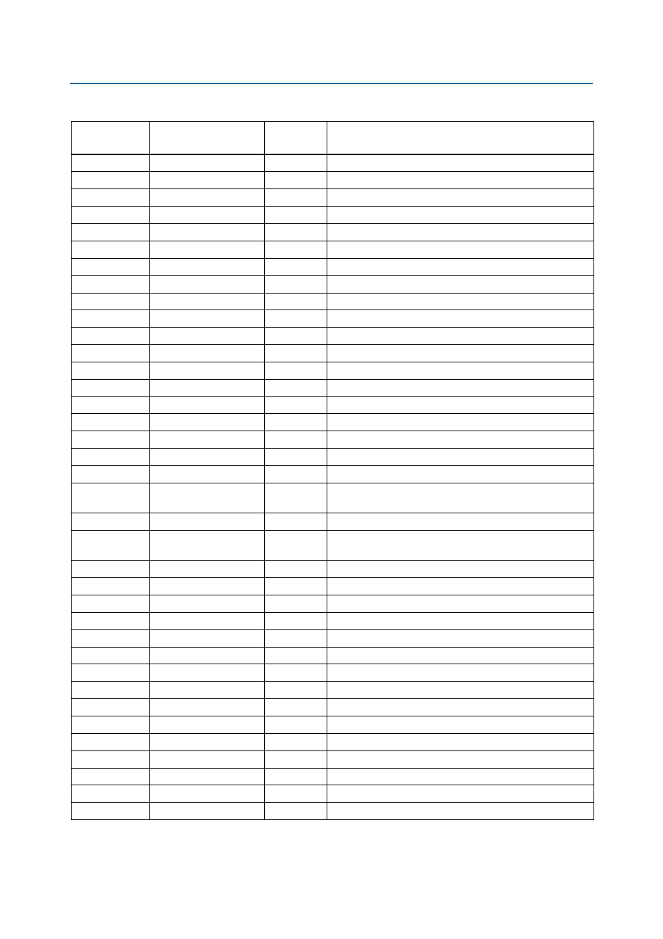
F6
FPGA_CONFIG_D13
2.5-V
FPGA configuration data
G2
FPGA_CONFIG_D14
2.5-V
FPGA configuration data
G3
FPGA_CONFIG_D15
2.5-V
FPGA configuration data
N3
FPGA_CVP_CONFDONE
2.5-V
FPGA Configuration via Protocol (CvP) done
J3
FPGA_DCLK
2.5-V
FPGA configuration clock
N1
FPGA_NCONFIG
2.5-V
FPGA configuration active
J4
FPGA_NSTATUS
2.5-V
FPGA configuration ready
H1
FPGA_PR_DONE
2.5-V
FPGA partial reconfiguration done
P2
FPGA_PR_ERROR
2.5-V
FPGA partial reconfiguration error
E2
FPGA_PR_READY
2.5-V
FPGA partial reconfiguration ready
F5
FPGA_PR_REQUEST
2.5-V
FPGA partial reconfiguration request
B11
HPS_RESETN
2.5-V
HPS reset push button
B8
HSMA_PRSNTN
2.5-V
HSMC port A present
M1
I2C_SCL_MAX
2.5-V
Programmable oscillator I
2
C clock
M2
I2C_SDA_MAX
2.5-V
Programmable oscillator I
2
C data
L6
JTAG_MAX_TDI
2.5-V
JTAG chain data in
M5
JTAG_MAX_TDO
2.5-V
JTAG chain data out
N4
JTAG_MAX_TMS
2.5-V
JTAG chain mode
P3
JTAG_MUX_TCK
2.5-V
JTAG chain clock
P11
M570_CLOCK
1.8-V
25-MHz clock to embedded USB-Blaster II for sending
FACTORY command
L5
M570_PCIE_JTAG_EN
2.5-V
M570 JTAG enable for the embedded USB-Blaster II
H2
MAX_AS_CONF
2.5-V
Driven low to enable AS configuration from the EPCQ flash
through U13 to the FPGA
E11
MAX_CONF_DONE
2.5-V
Embedded USB-Blaster II configuration done LED
A4
MAX_ERROR
2.5-V
FPGA configuration error LED
G4
MAX_FPGA_MISO
2.5-V
FPGA to MAX V SPI bus data output
G1
MAX_FPGA_MOSI
2.5-V
FPGA to MAX V SPI bus data input
H3
MAX_FPGA_SCK
2.5-V
FPGA to MAX V SPI bus clock
G5
MAX_FPGA_SSEL
2.5-V
FPGA to MAX V SPI bus slave select
A6
MAX_LOAD
2.5-V
FPGA configuration active LED
M9
MAX_RESETN
2.5-V
MAX V reset push button
B10
MSEL0
2.5-V
FPGA MSEL0 setting
B3
MSEL1
2.5-V
FPGA MSEL1 setting
C10
MSEL2
2.5-V
FPGA MSEL2 setting
C12
MSEL3
2.5-V
FPGA MSEL3 setting
C6
MSEL4
2.5-V
FPGA MSEL4 setting
E10
OVERTEMP
2.5-V
Temperature monitor fan enable
C7
PCIE_JTAG_EN
2.5-V
PCIe JTAG master enable
Table 2–4. MAX V CPLD System Controller Device Pin-Out (Part 3 of 4)
Board
Reference (U19)
Schematic Signal Name
I/O Standard
Description