Sdi video input, Memory, Sdi video input –37 – Altera Cyclone V SoC Development Board User Manual
Page 45: Memory –37
Chapter 2: Board Components
2–37
Memory
November 2013
Altera Corporation
Cyclone V SoC Development Board
Reference Manual
SDI Video Input
The cable equalizer supports operation at 270 Mb SD, 1.5 Gb HD, and 3.0 Gb dual-link
HD modes. The data rate is driven directly from the Cyclone V SoC transceiver
output using a slower-speed CMU channel (maximum of 3.125 Gbps). Control signals
are allowed for bypassing or disabling the device, as well as a carrier detect or auto-
mute signal interface.
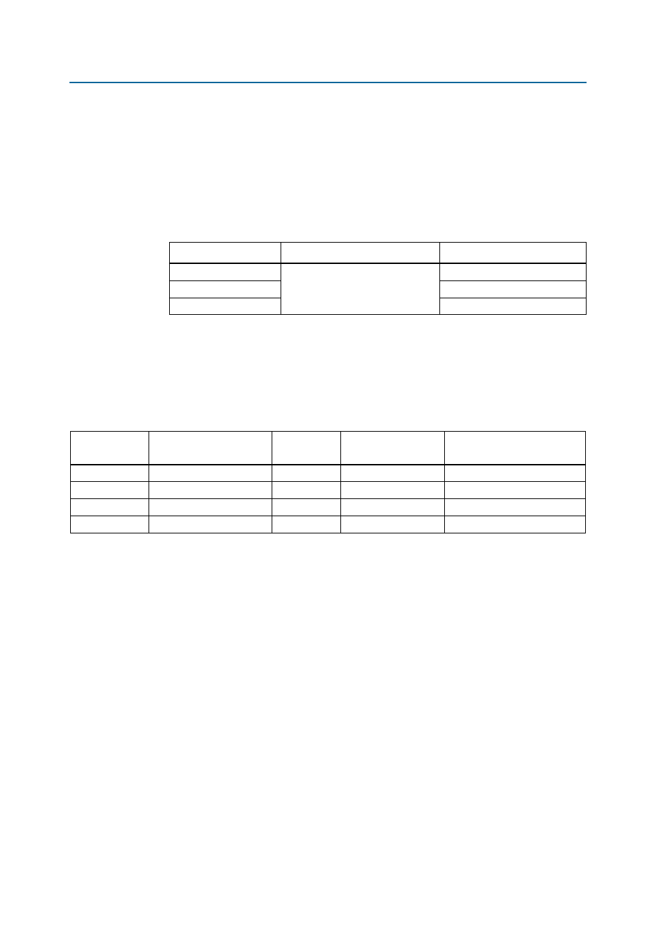
Table 2–30
shows the cable equalizer lengths.
f
For more information about the application circuit of the LMH0303 cable equalizer,
refer to the cable equalizer data sheet at
.
Table 2–31
summarizes the SDI video input interface pin assignments, signal names,
and functions.
Memory
This section describes the development board’s memory interface support and also
their signal names, types, and connectivity relative to the Cyclone V SoC. The
development board has the following memory interfaces:
■
DDR3 SDRAM (FPGA)
■
DDR3 SDRAM (HPS)
■
QSPI flash (HPS)
■
EPCQ flash
■
CFI flash
■
Micro SD flash memory
■
I
2
C EEPROM
f
For more information about the memory interfaces, refer to the following documents:
■
section in the External Memory Interface Handbook.
Table 2–30. SDI Cable Equalizer Lengths
Data Rate (Mbps)
Cable Type
Maximum Cable Length (m)
270
Belden 1694A
400
1485
140
2970
120
Table 2–31. SDI Video Input Interface Pin Assignments, Schematic Signal Names, and Functions
Board
Reference (U31)
Schematic Signal Name
I/O Standard
Cyclone V SoC Device
Pin Number
Description
7
SDI_RX_BYPASS
2.5-V
AB28
Equalizer bypass enable
14
SDI_RX_EN
2.5-V
AA28
Device enable
11
SDI_RX_P
1.5-V PCML
U2
SDI video output P
10
SDI_RX_N
1.5-V PCML
U1
SDI video output N