Fpga programming from flash memory, Fpga programming from flash memory –14 – Altera Cyclone V SoC Development Board User Manual
Page 22
2–14
Chapter 2: Board Components
FPGA Configuration
Cyclone V SoC Development Board
November 2013
Altera Corporation
Reference Manual
FPGA Programming from Flash Memory
Flash memory programming is possible through a variety of methods. The default
method is to use the factory design—Golden Hardware Reference Design. This design
contains an embedded webserver, which serves the Board Update Portal web
application. The web page allows you to link to SoC-related web pages and to control
some user I/O and LCD on the development board.
On either power-up or by pressing the program configuration push button,
PGM_CONFIG
(S12), the MAX V CPLD 5M2210 System Controller's PFL configures the
FPGA from the flash memory.
1
This feature is disabled by default. To enable this feature, slide the FACTORY_LOAD DIP
switch (SW2.3) to the ON position.
The PFL megafunction reads 16-bit data from the flash memory and converts it to fast
passive parallel (FPP) format. This 16-bit data is then written to the dedicated
configuration pins in the FPGA during configuration.
Pressing the PGM_CONFIG push button (S12) loads the FPGA with a hardware page
based on which PGM_LED[2:0] (D39, D40, D41) illuminates.
Table 2–6
lists the design that loads when you press the PGM_CONFIG push button.
B8
FX2_RESETN
K9
3.3-V
Embedded USB-Blaster hard reset
F3
FX2_SCL
J4
3.3-V
USB 2.0 PHY serial clock
G3
FX2_SDA
—
3.3-V
USB 2.0 PHY serial data
A1
FX2_SLRDN
K1
3.3-V
Read strobe for slave FIFO
B1
FX2_SLWRN
J9
3.3-V
Write strobe for slave FIFO
B7
FX2_WAKEUP
—
3.3-V
USB 2.0 PHY wake signal
G2
USB_B2_CLK
E2
3.3-V
USB 2.0 PHY 48-MHz interface clock
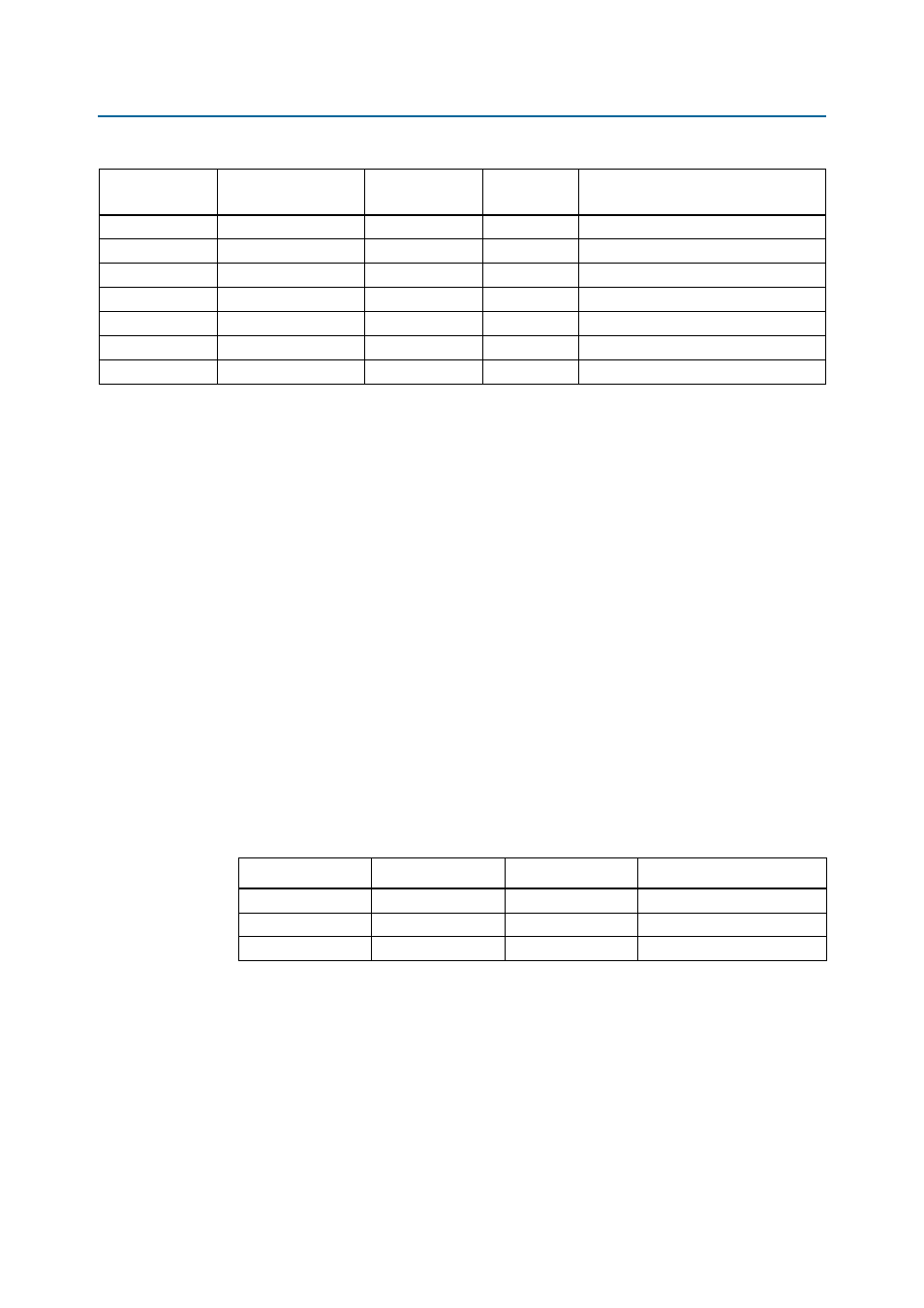
Table 2–5. USB 2.0 PHY Schematic Signal Names and Functions (Part 2 of 2)
Board Reference
(U51)
Schematic
Signal Name
MAX II CPLD Pin
Number
I/O Standard
Description
Table 2–6. PGM_LED Settings
(1)
PGM_LED0 (D41)
PGM_LED1 (D40)
PGM_LED2 (D39)
Design
ON
OFF
OFF
Factory hardware
OFF
ON
OFF
User hardware 1
OFF
OFF
ON
User hardware 2
Note to
Table 2–6
:
(1) ON indicates a setting of ’0’ while OFF indicates a setting of ’1’.