Off-board input/output clock, Off-board input/output clock –23 – Altera Cyclone V SoC Development Board User Manual
Page 31
Chapter 2: Board Components
2–23
Clock Circuitry
November 2013
Altera Corporation
Cyclone V SoC Development Board
Reference Manual
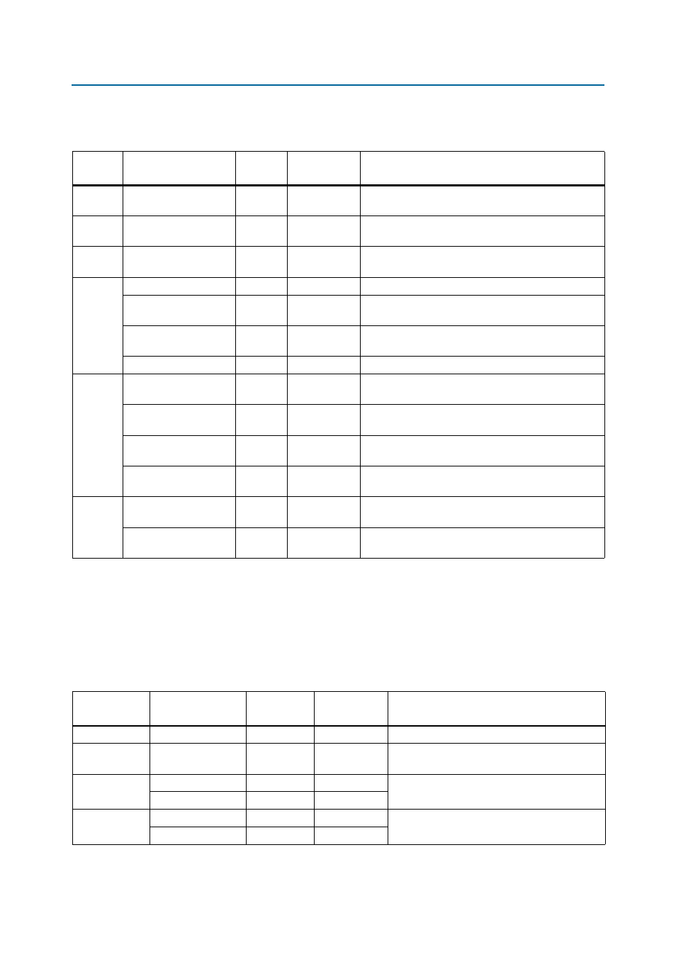
Table 2–16
lists the on-board clock inputs for the development board.
Off-Board Input/Output Clock
The development board has input and output clocks which can be driven onto the
board. The output clocks can be programmed to different levels and I/O standards
according to the FPGA device’s specification.
Table 2–16
lists the clock inputs for the development board.
Table 2–15. On-Board Clock Inputs
Source
Schematic Signal
Name
I/O
Standard
Cyclone V SoC
Pin Number
Description
X1
REFCLK_QL2_P
LVDS
P9
100 MHz programmable oscillator driving transceiver
bank QL2 REFCLK input for HSMA signals.
X3
CLK_148_P
LVTTL
T9
148.5 MHz programmable VCXO driving transceiver
bank QL1 REFCLK input for SDI video signals or SMA.
U49
PCIE_REFCLK_QL0_P
HSCL
W8
100 MHz fixed oscillator driving transceiver bank QL1
REFCLK input for PCI Express.
U35
CLK_ENET_FPGA_PHY
1.5-V
AA16
25 MHz fixed oscillator driving CLK2p in bank 4A
CLK_DUAL_ENET_PHY
1.5-V
—
25MHz fixed oscillator driving the Renesas dual
ethernet PHY (U45).
CLK_100M_MAX
1.5-V
—
100MHz fixed oscillator driving the MAX V CPLDpin J5
for FPGA configuration and other logic.
CLK_100M_FPGA
2.5-V
AB27
100 MHz fixed oscillator driving CLK5n in bank 5B.
U29
CLK_BOT1
1.5-V
AF14
100 MHz programmable oscillator driving CLK0p in
bank 3B for FPGA DDR3 or other logic.
CLK_TOP1
2.5-V
AA26
156.25 MHz programmable oscillator driving CLK5p in
Bank 5B.
CLK_OSC1
2.5-V
D25
25 MHz programmable oscillator driving HPS_CLK1 for
the HPS in bank 7A though SMA/XO multiplexer (U52).
CLK_OSC2
2.5-V
F25
25 MHz programmable oscillator driving HPS_CLK2 for
the HPS in bank 7A.
X4
CLK_50M_MAX
1.8-V
—
50 MHz fixed oscillator driving the MAX V CPLD pin
J12 for FPGA configuration or other logic.
CLK_50M_FPGA
1.5-V
AC18
50 MHz fixed oscillator driving CLK3p in bank 4A for
general logic.
Table 2–16. Off-Board Clock Inputs
Source
Schematic Signal
Name
I/O Standard
Cyclone V SoC
Pin Number
Description
SMA
CLKIN_SMA_HPS
2.5-V CMOS
—
Multiplexed clock input to OSC1 of the HPS
Samtec HSMC
HSMA_CLK_IN0
LVTTL
K14
Single-ended input from the installed HSMC
cable or board.
Samtec HSMC
HSMA_CLK_IN_P1
LVTTL
AG2
LVTTL input from the installed HSMC cable or
board.
HSMA_CLK_IN_N1
LVTTL
AH3
Samtec HSMC
HSMA_CLK_IN_P2
LVDS/LVTTL
H15
LVDS input from the installed HSMC cable or
board. Can also support 2x LVTTL inputs.
HSMA_CLK_IN_N2
LVDS/LVTTL
G15