Board overview, Board overview –2, Figure 2–1 – Altera Cyclone V SoC Development Board User Manual
Page 10: Table 2–1
2–2
Chapter 2: Board Components
Board Overview
Cyclone V SoC Development Board
November 2013
Altera Corporation
Reference Manual
Board Overview
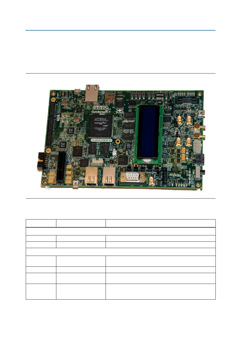
This section provides an overview of the Cyclone V SoC development board,
including an annotated board image and component descriptions.
shows
an overview of the board features.
describes the components and lists their corresponding board references.
Figure 2–1. Overview of the Cyclone V SoC Development Board Features
Table 2–1. Board Components (Part 1 of 3)
Board Reference
Type
Description
Featured Devices
U21
FPGA
Cyclone V SoC, 5CSXFC6D6F31C6, 896-pin FBGA.
U19
CPLD
MAX V CPLD, 5M2210ZF256I5N, 256-pin FBGA.
Configuration, Status, and Setup Elements
J23
JTAG chain header
Provides access to the JTAG chain and disables the embedded
USB-Blaster II when using an external USB-Blaster cable.
SW4
JTAG chain control DIP switch Remove or include devices in the active JTAG chain.
J37
Mini-USB header
USB interface for FPGA programming and debugging through the
embedded USB-Blaster II JTAG via a type-B USB cable.
SW2
Board settings DIP switch
Controls the MAX V CPLD 5M2210 System Controller functions such
as clock enable, SMA clock input control, and which image to load
from flash memory at power-up.