Jtag chain control dip switch, Fpga configuration mode dip switch – Altera Cyclone V SoC Development Board User Manual
Page 26
2–18
Chapter 2: Board Components
Setup Elements
Cyclone V SoC Development Board
November 2013
Altera Corporation
Reference Manual
JTAG Chain Control DIP Switch
The JTAG chain control DIP switch (SW4) either removes or includes devices in the
active JTAG chain.
Table 2–9
lists the switch controls and its descriptions.
FPGA Configuration Mode DIP Switch
The FPGA configuration mode DIP switch (SW3) defines the mode to use to configure
the FPGA.
lists the switch controls and its descriptions. All switches at the
ON position will select the default FPP x16 mode.
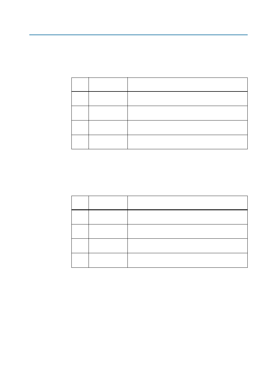
Table 2–9. JTAG Chain Control DIP Switch
Switch
Schematic Signal
Name
Description
1
HPS_JTAG_EN
ON: Bypass Cyclone V HPS in the chain
OFF: Cyclone V HPS in-chain
2
FPGA_JTAG_EN
ON: Bypass Cyclone V FPGA in the chain
OFF: Cyclone V FPGA in-chain
3
HSMA_JTAG_EN
ON: Bypass HSMC port in the chain
OFF: HSMC port in-chain
4
MAX_JTAG_EN
ON: Bypass MAX V CPLD 5M2210 System Controller in the chain
OFF: MAX V CPLD 5M2210 System Controller in-chain
Table 2–10. FPGA Configuration Mode DIP Switch
Switch
Schematic Signal
Name
Description
1
MSEL0
ON: Select logic 0
OFF: Select logic 1
2
MSEL1
ON: Select logic 0
OFF: Select logic 1
3
MSEL2
ON: Select logic 0
OFF: Select logic 1
4
MSEL3
ON: Select logic 0
OFF: Select logic 1