Altera Cyclone V SoC Development Board User Manual
Page 33
Chapter 2: Board Components
2–25
Components and Interfaces
November 2013
Altera Corporation
Cyclone V SoC Development Board
Reference Manual
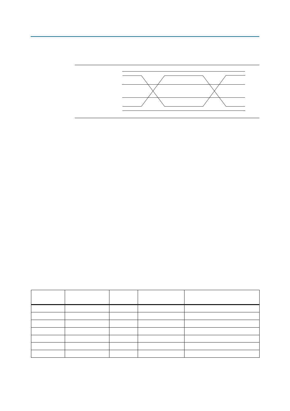
Figure 2–6
shows the PCI Express reference clock levels.
By default, the Cyclone V SoC development board is set up for the PCI Express
interface to use with the Cyclone V SoC device in root-port mode, such as when
plugging in a PCI Express add-in card into the PCI Express socket (J25). In this case,
the switching regulator generates and drives the clock to both the Cyclone V SoC
device and the add-in card.
To use the PCI Express interface with the Cyclone V SoC device in end-point mode,
for example, with a cable plugged into a PC, you must remove resistors R253, R254,
R249, and R251, and install R250 and R252. This resistor change will route the clock
from the PC directly into the Cyclone V SoC device. You can use a PCI Express gen1x4
cable from Samtec (HDR-172378-02-PCIEC) for this connection.
1
This cable connects power (3.3 V and 12 V) from the PC to the development board and
therefore the development board's power needs to be isolated to function properly. To
isolate the power, remove the development board's power isolation resistors, R554
and R547, located near the PCI Express connector. The ground pin (GND) will still
connect through the cable as it is required for normal operation.
The PCI Express edge connector also has a presence detect feature for the
motherboard to determine if a card is installed. A jumper is provided to optionally
connect PRSNT1n to any of the three PRSNT2n pins found within the x4 connector
definition. This is to address issues on some PC systems that would base the
link-width capability on the presence detect pins versus a query operation.
Table 2–18
summarizes the PCI Express pin assignments. The signal names and
directions are relative to the Cyclone V SoC.
Figure 2–6. PCI Express Reference Clock Levels
V
MAX
= 1.15 V
V
CROSS MAX
= 550 mV
V
CROSS MIN
= 250 mV
V
MIN
= –0.30 V
REFCLK –
REFCLK +
Table 2–18. PCI Express Pin Assignments, Schematic Signal Names, and Functions (Part 1 of 2)
Board
Reference (J18)
Schematic Signal
Name
I/O Standard
Cyclone V SoC Device
Pin Number
Description
A11
PCIE_PERSTN
LVTTL
AG6
Reset
B17
PCIE_PRSNT2N_X1
LVTTL
AD29
Presence detect DIP switch
B31
PCIE_PRSNT2N_X4
LVTTL
A11
Presence detect DIP switch
A14
PCIE_REFCLK_SYN_N
HCSL
W7
Motherboard reference clock
A13
PCIE_REFCLK_SYN_P
HCSL
W8
Motherboard reference clock
B5
PCIE_SMCLK
LVTTL
AE29
SMB clock
B6
PCIE_SMDAT
LVTTL
J14
SMB data