Max v reset push button, Program configuration push button, Program select push button – Altera Cyclone V SoC Development Board User Manual
Page 28: General user input/output, User-defined push buttons, General user input/output –20, User-defined push buttons –20
2–20
Chapter 2: Board Components
General User Input/Output
Cyclone V SoC Development Board
November 2013
Altera Corporation
Reference Manual
MAX V Reset Push Button
The MAX V reset push button, MAX_RESETn (S2), is an input to the MAX V CPLD
5M2210 System Controller. This push button is the default reset for the CPLD logic.
Program Configuration Push Button
The program configuration push button, PGM_CONFIG (S12), is an input to the MAX V
CPLD 5M2210 System Controller. This input forces a FPGA reconfiguration from the
flash memory. The location in the flash memory is based on the settings of
PGM_LED[2:0]
, which is controlled by the program select push button, PGM_SEL (S2).
Valid settings include PGM_LED0, PGM_LED1, or PGM_LED2 on the three pages in flash
memory reserved for FPGA designs.
Program Select Push Button
The program select push button, PGM_SEL (S11), is an input to the MAX V CPLD
System Controller. This push button toggles the PGM_LED[2:0]sequence that selects
which location in the flash memory is used to configure the FPGA. Refer to
Table 2–6
on page 2–14
for the PGM_LED[2:0] sequence definitions.
General User Input/Output
This section describes the user I/O interface to the FPGA, including the push buttons,
DIP switches, LEDs, expansion header, and character LCD.
User-Defined Push Buttons
The development board includes six user-defined push buttons. For information
about the system and safe reset push buttons, refer to
.
Board references S1–S6 are push buttons for controlling the FPGA designs that loads
into the Cyclone V SoC device. Push buttons S5 and S6 connect to the FPGA while
push buttons S1–S4 connect to the HPS. When you press and hold down the switch,
the device pin is set to logic 0; when you release the switch, the device pin is set to
logic 1. There are no board-specific functions for these general user push buttons.
Table 2–12
lists the user-defined push button schematic signal names and their
corresponding Cyclone V SoC pin numbers.
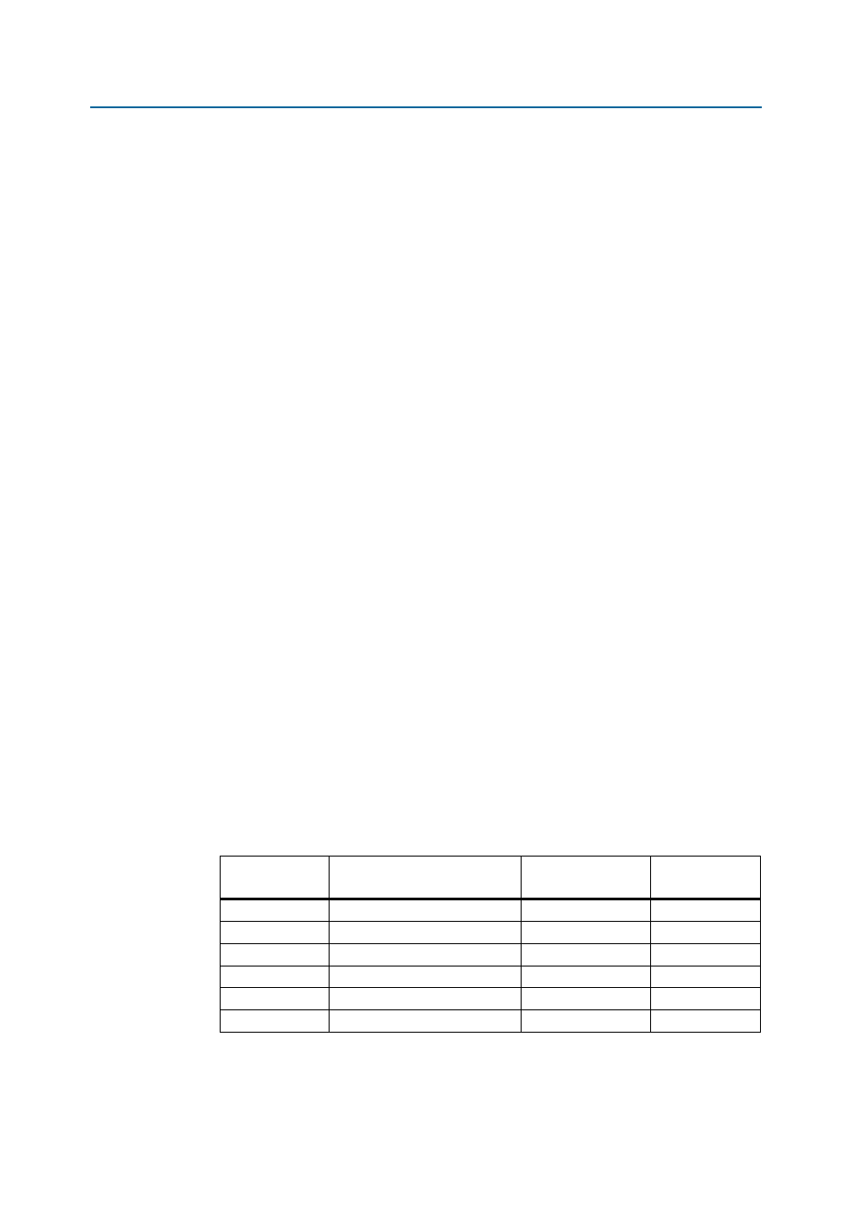
Table 2–12. User-Defined Push Button Schematic Signal Names and Functions
Board Reference
Schematic Signal Name
Cyclone V SoC Pin
Number
I/O Standard
S6
USER_PB_FPGA0
AA13
1.5-V
S5
USER_PB_FPGA1
AB13
1.5-V
S4
USER_PB_HPS0
T30
2.5-V
S3
USER_PB_HPS1
U28
2.5-V
S2
USER_PB_HPS2
T21
2.5-V
S1
USER_PB_HPS3
U20
2.5-V