Altera FIR Compiler User Manual
Page 6
1–2
Chapter 1: About the FIR Compiler
© May 2011
Altera Corporation
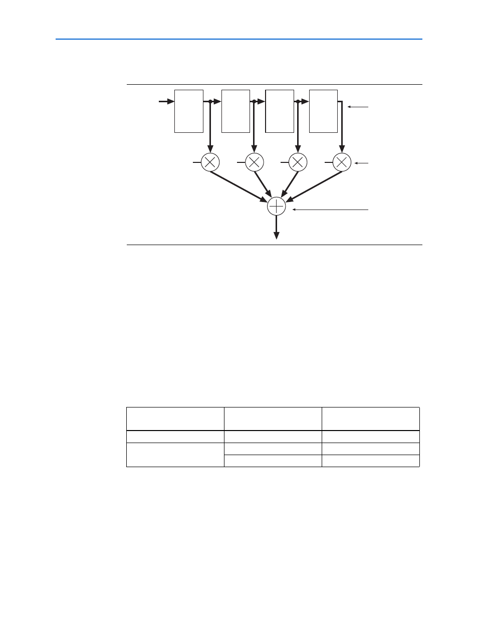
The structure of a FIR filter is a weighted, tapped delay line as shown in
.
The filter design process involves identifying coefficients that match the frequency
response specified for the system. These coefficients determine the response of the
filter. You can change the signal frequencies that pass through the filter by changing
the coefficient values or adding more coefficients.
DSP processors have a limited number of multiply accumulators (MACs), and require
many clock cycles to compute each output value (the number of cycles is directly
related to the order of the filter).
A dedicated hardware solution can achieve one output per clock cycle. A fully
parallel, pipelined FIR filter implemented in an FPGA can operate at very high data
rates, making FPGAs ideal for high-speed filtering applications.
compares resource usage and performance for different implementations of
a 120-tap FIR filter with a 12-bit data input bus.
The Altera FIR Compiler speeds the design cycle by:
■
Generating the coefficients needed to design custom FIR filters.
■
Generating bit-accurate and clock-cycle-accurate FIR filter models (also known as
bit-true models) in the Verilog HDL and VHDL languages and in the MATLAB
environment.
Figure 1–2. Basic FIR Filter
Table 1–1. FIR Filter Implementation Comparison
Device
Implementation
Clock Cycles to
Compute Result
DSP processor
1 MAC
120
FPGA
1 serial filter
12
1 parallel filter
1
Note to
:
(1) If you use the FIR Compiler to create a filter, you can also implement a variable filter in a FPGA that uses from 1
to 120 MACs, and 120 to 1 clock cycles.
xin
yout
Z
-1
Z
-1
Z
-1
Z
-1
C
0
C
1
C
2
C
3
Tapped
Delay Line
Coefficient
Multipliers
Adder Tree