Rx latency, Serial port interface (spi) – Altera JESD204B IP User Manual
Page 117
RX Latency
The RX latency is defined as the time needed to fully transfer a 32-bit data in a lane
(
jesd204_rx_link_datain*
) to the Avalon-ST interface (
jesd204_rx_dataout*
) when the
jesd204_rx_link_data_valid
signal equals to "1".
Table 5-17: RX Latency Associated with Different F and FRAMECLK_DIV Settings.
F
FRAMECLK_DIV
RX Latency
1
1
• Maximum 5
rxframe_clk
period for byte 3
• Minimum 2
rxframe_clk
period for byte 0
1
4
2
rxframe_clk
period
2
1
• Maximum 3
rxframe_clk
period for byte 2 and byte 3
• Minimum 2
rxframe_clk
period for byte 0 and byte 1
2
2
2
txframe_clk
period
4
—
2
txframe_clk
period
8
—
2
txframe_clk
period
Serial Port Interface (SPI)
An external converter device with a SPI allows you to configure the converter for specific functions or
operations through a structured register space provided inside the converter device. The SPI gives
flexibility and customization, depending on the application. Addresses are accessed via the serial port and
can be written to or read from the port. The memory is organized into bytes that can be further divided
into fields.
The SPI communicates using two data lines, a control line, and a synchronization clock. A single SPI
master can work with multiple slaves. The SPI core logic is synchronous to the clock input provided by
the Avalon-MM interface. When configured as a master, the core divides the Avalon-MM clock to
generate the
SCLK
output.
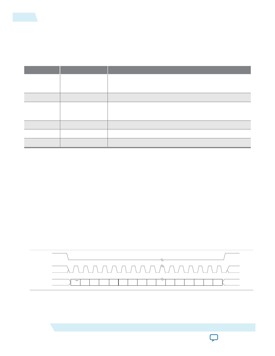
Figure 5-13: Serial Port Interface (24-bit) Timing Diagram
Figure shows the timing diagram of a 24-bit SPI transaction required by a typical external converter
device.
R/W W1
W0
A12
A11
A10
A9
A8
A7
D5
D4
D3
D2
D1
D0
Don’t Care
Don’t Care
Don’t Care
Don’t Care
SS_n
SCLK
SDIO
The first 16 bits are instruction data. The first bit in the stream is the read or write indicator bit. This bit
goes high to indicate a read request. W1 and W0 represent the number of data bytes to transfer for either
a read or write process. For implementation simplicity, W1 and W0 are always set at 0 in this design
5-36
RX Latency
UG-01142
2015.05.04
Altera Corporation
JESD204B IP Core Design Guidelines