Figure 3-30: data transfer on the i2c bus – ADLINK PCIe-7360 User Manual
Page 73
Operations
63
PCIe-7360
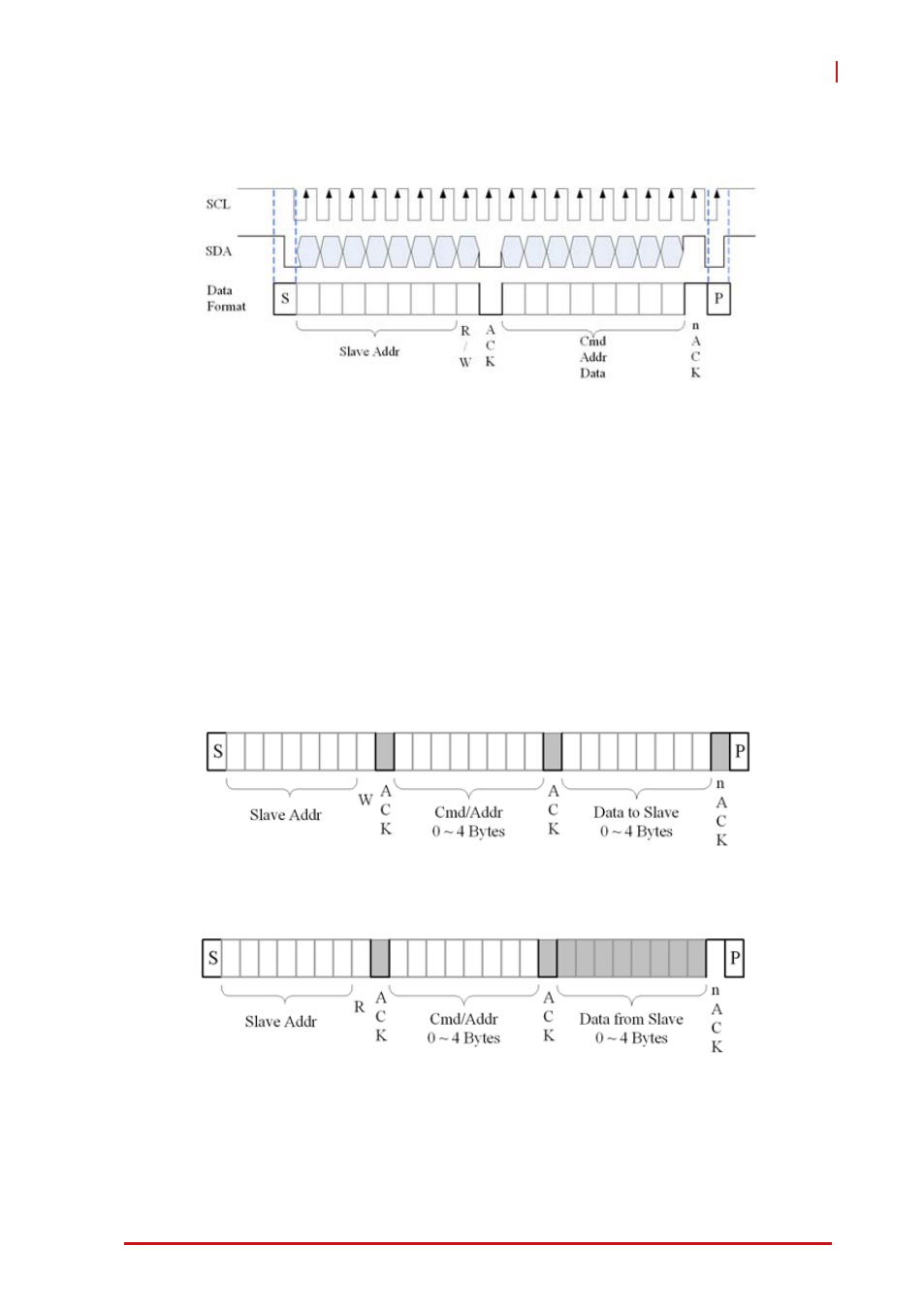
Address or Data). Figure 3-29 shows the data transfer on the I
2
C
bus.
Figure 3-30: Data Transfer on the I
2
C Bus
I
2
C master of PCIe-7360 supports the clock range from 1.9 kHz to
244.14 kHz. After issuing command to I
2
C slave device, the clock
rate might be changed according the request from I
2
C slave. The
below formula is to calculate the I
2
C clock rate.
F
scl
= 488.28 / (Clk Pre-scale + 1) (kHz),
where Clk Pre-scale = 1 to 255
I
2
C Write Command: the content of Cmd/Addr and Data are
stored in registers I
2
C_A_CA and I
2
C_A_DAT and their byte
counts are indicated by I
2
C CmdAddr Byte Count and Access Byte
Count, respectively.
I
2
C Read Command: the format of Read command is similar with
a write command except that the data part is derived by slave
device.
- USB-1901 (84 pages)
- USB-1210 (54 pages)
- USB-2401 (60 pages)
- USB-7230 (50 pages)
- USB-2405 (56 pages)
- DAQe-2010 (92 pages)
- DAQe-2204 (100 pages)
- DAQe-2213 (94 pages)
- DAQe-2501 (74 pages)
- PXI-2010 (84 pages)
- PXI-2020 (60 pages)
- PXI-2501 (62 pages)
- cPCI-9116 (98 pages)
- ACL-8112 Series (94 pages)
- ACL-8112 Series (92 pages)
- ACL-8112 Series (93 pages)
- ACL-8216 (75 pages)
- ACL-8111 (61 pages)
- PCM-9112+ (10 pages)
- PCM-9112+ (94 pages)
- cPCI-6216V (47 pages)
- ACL-6126 (28 pages)
- ACL-6128A (40 pages)
- PCM-6308V+ (52 pages)
- PCM-6308V+ (4 pages)
- PCI-7444 (82 pages)
- PCI-7434 (48 pages)
- PCI-7234 (56 pages)
- PCI-7260 (66 pages)
- PCI-7258 (38 pages)
- PCI-7256 (48 pages)
- PCI-7250 (48 pages)
- LPCI-7250 (48 pages)
- PCI-7396 (65 pages)
- PCI-7296 (59 pages)
- PCI-8554 (67 pages)
- PCIe-7350 (86 pages)
- PCIe-7300A (114 pages)
- PCIe-7200 (51 pages)
- PCI-7300A (112 pages)
- PCI-7300A (83 pages)
- PCI-7200 (96 pages)
- cPCI-7300 (82 pages)
- cPCI-7300 (83 pages)