5 bus-mastering dma data transfer, Bus-mastering dma data transfer, Figure 3-7: maximum data throughput – ADLINK PCIe-7360 User Manual
Page 39
Operations
29
PCIe-7360
3.5 Bus-mastering DMA Data Transfer
Digital I/O data transfer between PCIe-7360 and PC’s system
memory is through bus mastering DMA, which is controlled by
PCIe IP Core.
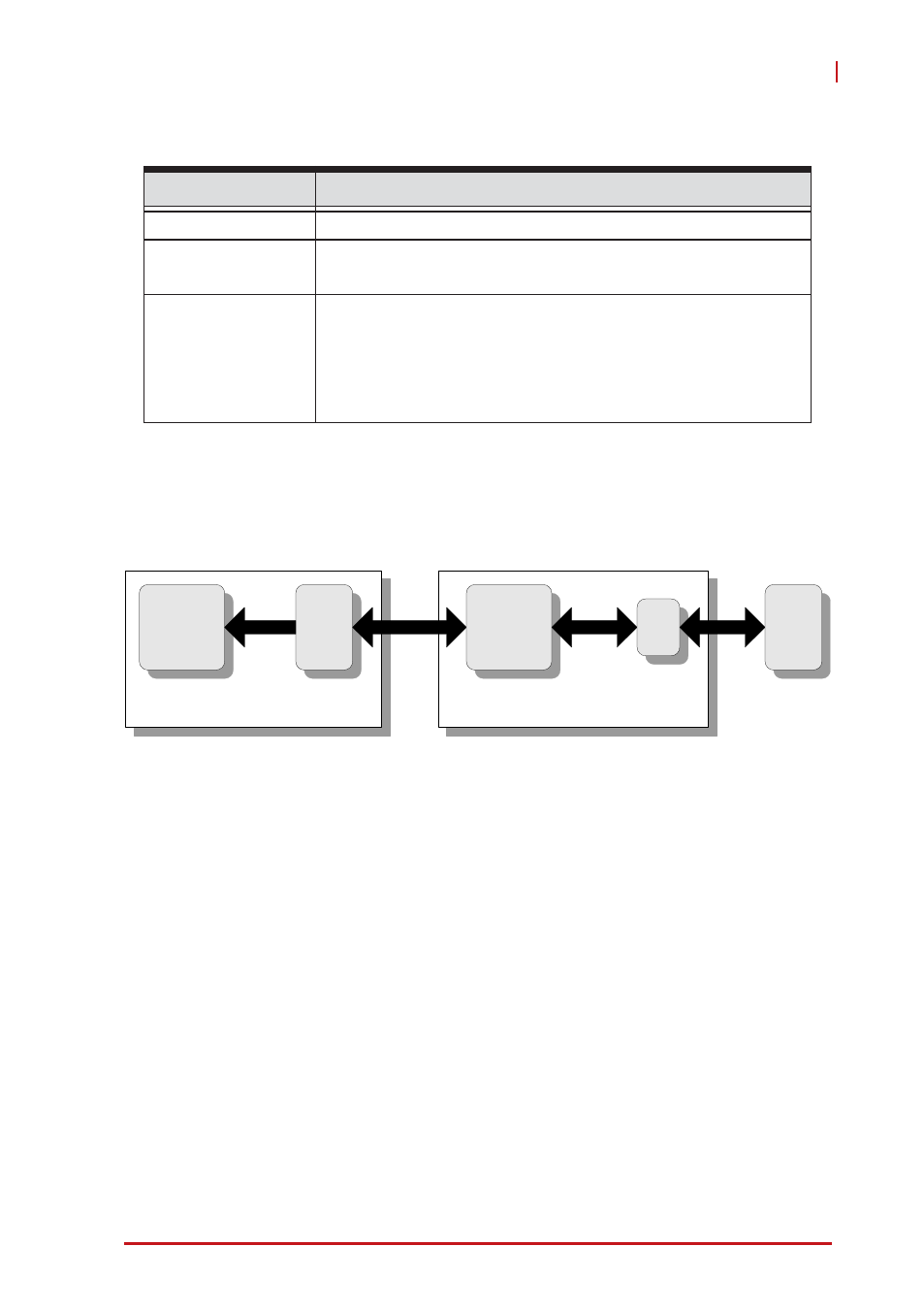
Figure 3-7: Maximum Data Throughput
The bus-mastering controller controls the PCI/PCIe bus when it
becomes the master of the bus. Bus mastering reduces the size of
the on-board memory and reduces the CPU loading because data
is directly transferred to the computer’s memory without host CPU
intervention.
Bus-mastering DMA provides the fastest data transfer rate on the
PCI/PCIe bus. Once the analog/digital input operation starts, con-
trol is returned to the program. The hardware temporarily stores
the acquired data in the onboard Data FIFO and then transfers the
data to a user-defined DMA buffer memory in the computer.
Please note that even when the acquired data length is less than
the Data FIFO, the data will not be kept in the Data FIFO but
directly transferred into host memory by the bus-mastering DMA.
Value
Revolution
80 steps (1 step = 4.5°)
Supported
Frequency Range
20 MHz to 100MHz
Supported CLK
User can shift the clock phase ofthe following clock:
External DI sample clock (from SMB CLK IN or AFI7)
External DO sample clock (from SMB CLK IN or AFI6)
Exported DI sample clock (from SMB CLK IN or AFI7)
Exported DO sample clock (from SMB CLK IN or AFI6)
System
Memory
NB
Chipset
500 MB/s
PC Mainboard
PCI-
Express
IP Core
FIFO
500MB/s
DUT
PCIe-7360